Jump To: PCBA Terminology | Through-Hole Assembly | Surface Mount Technology | Mixed Technology | PCB Manufacturing at Millennium Circuits Limited
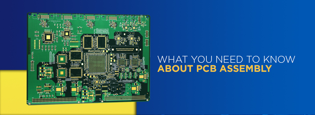
The printed circuit board (PCB) assembly process consists of various steps and guidelines that must be performed in the proper sequence for the finished product to function as designed. To ensure that this happens, PCB manufacturers use screen templates and controlled heating and cooling mechanisms to regulate how components are applied and fastened into place.
When you assemble a printed circuit board, you must choose the right technology for the type of components at hand. All of the parts and pieces must be correctly aligned in their designated spot, as specified in the PCB design. Any deviation, ever so slight, can have huge ramifications on the functions of the finished board.
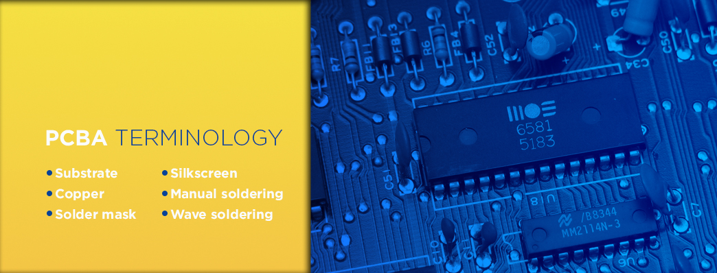
PCBA Terminology
To understand the PCB assembly process, you need to know the meaning of several terms:
- Substrate: The foundational material of the printed circuit board, the substrate makes each board firm and rigid.
- Copper: Each working side of a PCB contains a thin layer of copper, for conductive purposes. On single-layer boards, copper is placed on the active side. On double-sided PCBs, copper appears on both sides.
- Solder mask: This is the layer at the surface (typically green) of every printed circuit board. Solder mask provides insulation between copper and other materials, preventing shorts that could otherwise occur if different conductive materials come into contact. Solder mask provides structure for the layout of the PCB by keeping everything in its place. Each board contains holes that go through the solder mask. Solder is placed within each hole, which offers a foundation for each component that gets added to the board.
- Silkscreen: The final touch on every printed circuit board is the silkscreen, a transparent layer that displays numbers and letters next to the different parts of a given board. This allows manufacturers to identify the specific components of each board.
- Manual soldering: This is a process where a technician manually inserts a single component onto its designated spot on a series of printed circuit boards. Once completed, each board is sent to the next technician, who adds another part and passes the board onward.
- Wave soldering: Wave soldering involves correctly soldering where the board is placed on a conveyor and run through a heating chamber. Here, a wave of solder is applied to the bottom, fastening all the underpins of the board into place in a single process.
It is also important to understand the differences between through-hole, surface mount and mixed technology assemblies.
Through-Hole PCB Assembly
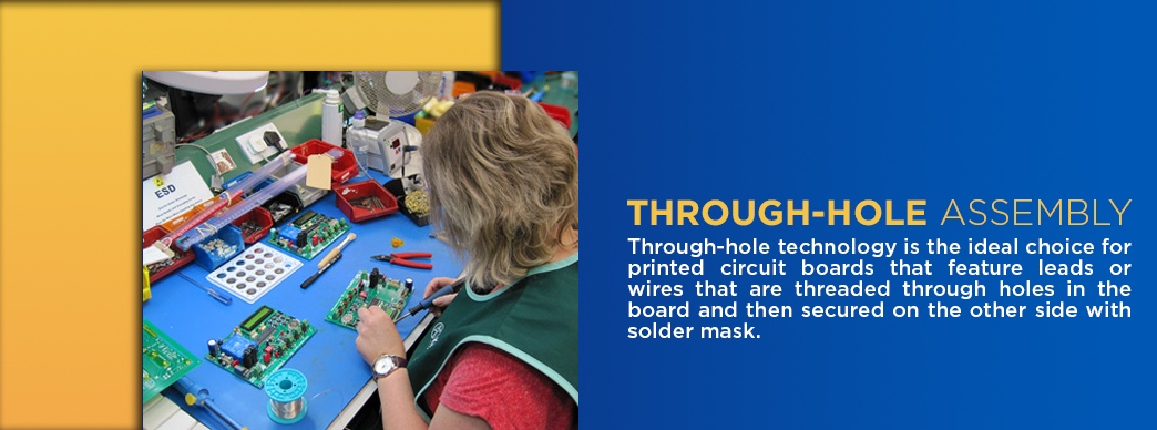
Through-hole technology is the ideal choice for printed circuit boards that feature leads or wires that are threaded through holes in the board and then secured on the other side with solder. PCBs with large components are especially suited to through-hole technology, especially capacitors.
The basic steps of through-hole PCB technology can be summarized as follows:
- The technician manually assembles parts onto specific areas on a printed circuit board, according to the design specifications of the PCB. Each component must be set in an exact position, as specified, for the PCB to function properly.
- The board is examined to ensure that all the parts have been properly assembled and that each component is set in its exact place. If any of the PCB parts are misplaced, now is the time to correct those imperfections.
- The components are now soldered into place on the circuit board. This is typically done with wave soldering, where the board moves above a wave of hot solder liquid which solidifies the PCB assembly. This can also be done by hand or by using selective solder. Selective solder is similar to wave soldering, however, the operator can solder areas selectively and this helps when you don’t want solder on certain areas.
Through-hole boards typically contain components with wire leads, either axial or radial. Compared to surface mount technology, through-hole boards generally feature stronger bonds. However, more work is required to produce a through-hole assembly because of the additional drilling involved.
If a through-hole board consists of multiple layers, signal traces have limited routing on the internal layers because the holes cut through between the top and bottom surfaces. Therefore, through-hole technology is often restricted to some of the bulkier PCB components like electrolytic capacitors and semiconductors. Boards that require additional firmness and support, such as electromechanical relays and plug connectors, are also made with through-hole technology.
During the prototyping stage, technicians often favor the bigger through-hole to the surface mount because the former works more readily with breadboard sockets. However, if a board is intended for high-speed or high-frequency purposes, the design might require surface mount technology to reduce stray reluctance. Otherwise, the function of the circuits would be degraded due to inductance or capacitance in the leads.
During the application of solder paste, a solder stencil is placed on top of the printed circuit board to ensure that the solder stays within the limits specified in the design. The stencil is a thin replica of the original design with cutouts for the areas where the components are placed.
Once the components have been set into place and the board has undergone its first inspection, the solder paste is heated over a hot liquid until the tiny metal balls within the paste solidify with the bonding chemical, flux. This bonds the components to the board permanently. After the heating and bonding have finished, the board is cooled in a controlled setting. This brings the board back to a normal state and prevents shock.
Now complete, the printed circuit board must have its components examined for any possible misalignments. If the components are relatively large, this can often be done with a visual inspection. These days, however, optical and x-ray inspectors can examine PCBs with much higher accuracy. If design flaws are detected, the problem must be fixed before more boards go through the process.
Surface Mount Technology
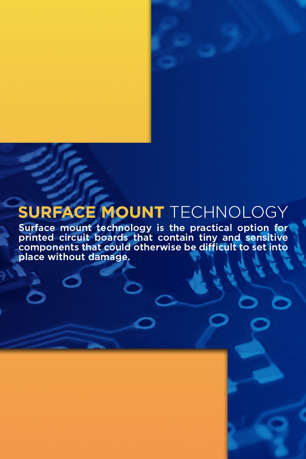
Surface mount technology is the practical option for printed circuit boards that contain tiny and sensitive components that could otherwise be difficult to set into place without damage. Examples of the kind of components that undergo this process include diodes and resistors.
The basic steps of surface-mount technology can be summarized as follows:
- The first step involves a printer designed for the application of solder paste. A solder screen template is used to ensure that the tiny components are put into their proper places. Before the components are actually placed, the stencil is inspected to make sure that the template is aligned correctly.
- The board is now taken to a machine where the components are put into place according to the design of the solder screen template. Reels in the machine ensure that the parts are aligned and attached to their corresponding pads.
- With the components properly set on the board, a heating process is employed to solidify everything into place. At this stage, the PCB is sent through a heating chamber that liquefies the solder, fastening the parts in the process.
Before the components are placed onto a PCB, select areas of the board itself must first be coated with solder paste, which functions as the adhesive for the unique parts of the board. The areas that require solder are primarily the spots where pads will exist for the corresponding components.
Solder paste is made of tiny grains and flux. The process of placing the solder paste onto a printed circuit board is much like that of a printing application. A solder screen is set over the board to an exact, specified alignment. A roller is then run over the screen to press the solder paste onto the board.
The solder screen is printed in advance according to the design of the PCB. Therefore, the aperture in the screen are aligned to the component pads on the board. This ensures that the solder mask distributes exclusively on those areas. The quantity of solder distributed during this process must be regulated to ensure that each joint is neither over-covered or under-covered.
Once the paste has been applied, the board is sent through a pick-and-place machine where specified components are applied to the soldered areas. As long as external forces do not jolt the board during this process, the tension of the solder should be sufficient to hold the components in place.
On some pick-and-place machines, tiny amounts of adhesive are added to the designated areas to secure the components. This is mainly intended for printed circuit boards that undergo the process of wave soldering. The drawback of this added adhesive is that it can make corrections difficult on boards where the components have been misaligned to the specs of the original design.
With the components secured to their proper spots, the PCB is sent through the soldering machine. On older boards, manufacturers often employed wave soldering, though this has largely been taken out of practice. In productions where the method is employed, solder paste is not used because solder is applied by the wave soldering machine. Today, however, reflow soldering is the more commonly used method among PCB manufacturers.
Once the printed circuit board has come out of the soldering machine, technicians inspect the board’s composition for any imperfections. If the board contains more than 100 different components, the board is sent through an automatic optical inspector (AOI), which can detect even the slightest flaws, such as misaligned joints, off-place components and incorrect placements.
Each printed circuit board must undergo a series of tests before it leaves the assembly. The board endures several tests to verify that it can function as intended in the original design.
While the operation is in progress, the equipment must be inspected to ensure that everything works as intended. The first places to check are the outputs, as these will help verify the success of a given production. The output of the soldering machine should be inspected at the start of each production, along with the initial boards that come through the output. This way, any imperfections can be caught early, before a misprinting error becomes large and costly.
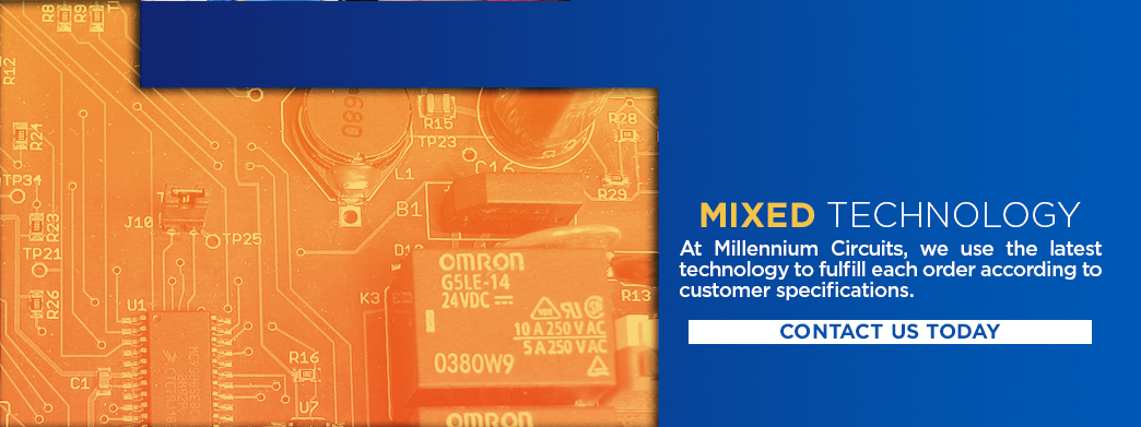
Mixed Technology
Due to the rapid evolution of computerized technology, an increasing number of printed circuit boards are being made with smaller and smaller parts. This means many PCBs are made today with a combination of methods, commonly referred to as mixed technology. An assembly that involves mixed technology will encompass one of the following approaches:
- A single-sided mixed assembly, where a printed circuit board undergoes surface mount technology as well as through-hole technology, both on the same side of the board.
- A split assembly, where one side of the printed circuit board is assembled with surface mount technology and the other side of the board is assembled with through-hole technology. PCBs like these have normal-size components on one side and tinier components on the other side.
- A double-sided mixed assembly, where both sides of the printed circuit board are assembled with a combination of through-hole technology and surface mount-technology. A board of this type features regular components as well as tiny and delicate ones on both sides.
Before a PCB design goes into production, the boards intended for use must be inspected for quality purposes. On the components, foot oxidation or oily residue could serve as red flags. If stored in a cool environment, the solder paste can only be applied once it has been thawed and stirred. The PCB must be dry before any paste is applied to the surface.
On printed circuit boards with mixed technology, a more complex set of processes are required within the pick-and-place machine. Here, a mixture of different component sizes will need to be accounted for, either on one or both sides of the board.
If the printed circuit board consists of a double-sided assembly, the soldering process will need to be applied to both sides. Basically, everything that happens on one side also happens on the other. The only difference is the specific components and their placements, as one side might contain smaller components than the other. Wave soldering is not possible for two-sided PCBs because resubmitting the board for the second side would ruin the delicate parts on the first side.
Any printed circuit board comprised of mixed technology should be submitted to an automatic optical inspector. This way, technicians can be ensured a foolproof inspection that will detect even the tiniest imperfections, such as minor misplacements of microscopic parts.
To account for the complexities of a two-sided mixed technology board, a more thorough set of tests are required for the initial PCBs produced in such lines. Since there are more components to account for, there are more potential problems if even one part is out of alignment.
PCB Manufacturing at Millennium Circuits Limited
In today’s high-tech world, printed circuit boards are becoming increasingly complex as technicians find ways to load more data and energy onto tinier and tinier chips. As computer devices and electronics become smaller, so too will the PCBs that power these devices and connect them to the wireless grid. For PCB manufacturers, this means that the production of printed circuit boards will require advanced levels of engineering.
To make PCBs efficient by current standards, you must have the proper specified bare PCB to carry out each step more efficiently in the assembly process. At Millennium Circuits, we use the latest technology at our facilities to fulfill each bare PCB order according to customer specifications. Contact Millennium Circuits for more information about PCB manufacturing.
Do you have questions about our services or your project? Contact us today to speak with MCL’s award-winning support team!
![]()