

Advanced PCB Manufacturing for Next-Generation Electronic Designs
As electronic devices continue to evolve, engineers are being challenged to fit more performance into smaller spaces. Higher data rates, increased routing density, tighter signal integrity requirements, and advanced packaging technologies are pushing conventional PCB fabrication to its limits.
When traditional manufacturing methods can no longer support your design objectives, MCL helps you move forward.
Through our global manufacturing network and engineering expertise, MCL provides access to Modified Semi-Additive Process (MSAP) technology—an advanced PCB manufacturing process that enables ultra-fine features, higher circuit density, and improved performance for today’s most demanding applications.
Whether you’re developing AI infrastructure, high-speed networking equipment, medical devices, or next-generation computing platforms, our engineering team works with you to determine if MSAP is the right manufacturing solution for your design.
Get Pricing and Lead Time Call 717-558-5975
What is MSAP?
Modified Semi-Additive Process (MSAP) is an advanced PCB manufacturing process designed to produce significantly finer trace widths and spacing than conventional subtractive etching.
Instead of removing copper from a laminate to create circuit patterns, MSAP builds copper only where it’s needed. This approach enables much tighter geometries while improving precision and supporting increasingly complex PCB designs.
The result is greater routing density, improved electrical performance, and more design flexibility without increasing board size.

Why Engineers Choose MSAP 
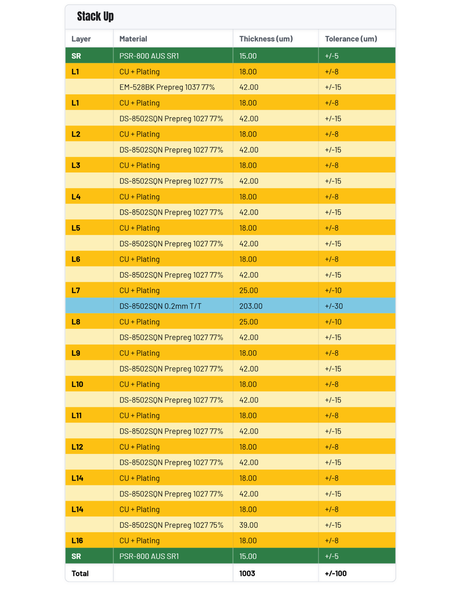
As PCB designs become more complex, engineers often face limitations that conventional fabrication cannot efficiently overcome.
MSAP can help address challenges such as:
- Ultra-fine trace widths and spacing
- Higher routing density
- Increased signal integrity requirements
- Board miniaturization
- High-speed data transmission
- Complex HDI architectures
- Advanced packaging applications
Rather than increasing board size or adding additional layers, MSAP allows more circuitry to fit within the same footprint, giving engineers greater design flexibility.
Benefits of MSAP Technology
- Greater Routing Density: Fit more routing into the same PCB area while supporting increasingly complex electronic designs.
- Improved Signal Integrity: Finer geometries can help support impedance control, reduce signal loss, and improve high-speed electrical performance.
- Potential Layer Count Reduction: By creating additional routing space, some designs may achieve required performance with fewer PCB layers, helping simplify manufacturing while reducing overall system complexity.
- Enhanced Miniaturization: Enable more functionality in smaller form factors for space-constrained applications.
- Supports Future Technologies: MSAP helps support emerging technologies requiring higher bandwidth, increased circuit density, and improved electrical performance.
Applications
MSAP is particularly valuable for advanced electronic applications, including:
- Artificial Intelligence (AI) Infrastructure
- High-Performance Computing (HPC)
- High-Speed Networking
- Data Center Equipment
- Optical Networking
- Silicon Photonics
- Medical Devices
- Aerospace & Defense Electronics
- Wearable Technology
- RF & Microwave Applications
Request a free quote today.

Is MSAP Right for Your Design?
Not every PCB requires MSAP.
At MCL, we don’t recommend advanced manufacturing technologies unless they provide a clear advantage for your application.
Our engineering team reviews each project individually, evaluating factors such as:
- Routing density
- Signal integrity requirements
- Layer count
- Thermal considerations
- Manufacturability
- Long-term production goals
For many designs, conventional PCB fabrication remains the right solution. When greater precision or routing capability is needed, MSAP may provide the performance your project requires.
Designed for High-Speed Data Transmission
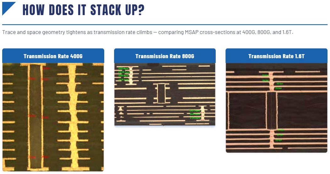
MCL supports advanced PCB designs for 400G, 800G, and 1.6T optical applications, helping enable the signal integrity and routing density required as next-generation data transmission speeds increase.

WHY MCL?
When requirements are demanding and timelines are tight, you don’t just need boards. You need a partner who executes.
We work with your team early to understand requirements, identify potential challenges, and recommend the right path forward. From DFM and stackup guidance to manufacturing technology and sourcing strategy, we help you navigate the decisions that can impact cost, quality, and schedule.
Whether your design calls for conventional fabrication, HDI, or advanced technologies like MSAP, we coordinate the right resources and manufacturing capabilities to keep your program on track.
Because demanding PCB programs don’t just need a supplier that can quote a board. They need a partner who owns the outcome.