Updated on March 17, 2025
Table of Contents:
- The PCB Manufacturing Process
- Types of Printed Circuit Board Design
- The History of PCB Production and Fabrication
- What Are the Parts of a PCB?
- How Are PCBs Made?
- The PCB Manufacturing Process for Multilayer Designs
- How to Implement an Effective PCB Manufacturing Process
Printed circuit boards (PCBs) are the backbone of modern electronics. They route electrical signals between all of the attached electronic components, bringing them to life.
Electronic devices or components can only function as intended with high-quality PCBs. As technology continues to evolve and consumers demand more from their electronics, manufacturers benefit from understanding how printed circuit boards are manufactured. The global PCB market is expected to reach $107.6 billion by 2030 as more organizations are manufacturing circuit boards.
 The PCB Manufacturing Process
 The
The A printed circuit board, or PCB, is a non-conductive material with conductive lines, also called traces, printed or etched into the base. Electrical components are mounted on the board, with traces connecting the components to form a working circuit. Most electrical devices use PCBs to provide physical and mechanical support.
The industrial PCB manufacturing process comprises many steps, checks, and balances to ensure the finished product performs as intended. Circuit boards can be single, double, or multilayered, but their construction only differs after producing the first layer. Many PCBs differ in their core structure, and could require more than 20 manufacturing steps to complete.
Types of Printed Circuit Board Design
Designers classify various PCB types based on design specifications, manufacturing processes, and applications. The most common types of PCBs include:
Single-Sided PCBs
The most common type of PCB is single-sided. It has a conductive copper layer above the substrate, and the electrical components are placed on one side of the board, leaving the entire etched circuit visible on the other. Because these boards have a single conductive layer, the conductive paths cannot overlap, which takes up additional space.
These PCBs are best suited to low-density design requirements and are often used for basic and low-cost electronic instruments. They are cost-effective and relatively easy to design, manufacture and repair.
Double-Sided PCBs
Double-sided PCBs feature a thin layer of conducting material on the top and bottom sides of the board. Holes in the board allow the traces and component pins to be connected from one side to the other. Manufacturers can use two mounting methods to connect the circuits on either side.
This type of PCB has several advantages, including reduced size for more compact circuits, cost-effectiveness, and increased circuit density, making it suitable for advanced electronic systems.
Multilayered PCBs
These PCBs have more than two copper layers. Their design resembles a sandwich, with several conductive layers divided by insulating material sheets. The layers must be bonded and laminated together under high pressure and temperatures to remove air gaps and keep the PCB assembly stable. They are suitable for high-speed circuits as they are more compact than single or double-sided options and have high design flexibility and complexity.
Rigid PCBs
Rigid PCBs have a solid substrate material, which gives the board rigidity and strength, and prevents twisting or folding. They consist of multiple layers, including:
- Substrate
- Copper
- Solder mask
- Silkscreen printed ink for component placement orientation and servicing
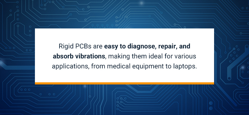
These layers are bonded together with a mixture of adhesive and heat. Rigid PCBs are easy to diagnose, repair, and absorb vibrations, making them ideal for various applications, from medical equipment to laptops.
Flex PCBs
Flex PCBs comprise multiple printed circuits and components arranged on a flexible substrate such as polyamide, polyether ether ketone (PEEK), or a transparent conductive polyester film. Their design allows them to flex to the desired form during application. They’re available in single-sided, double-sided, and multilayer options. In addition to their flexibility, these boards are compact, highly reliable, and repeatable, making them suitable for high signal trace density applications.
The History of PCB Production and Fabrication
German inventor Albert Hansen filed the first patent for a rudimentary PCB in 1903, and more complex patents followed. In the past half-century alone, we’ve experienced increased functionality on a micro level, allowing smaller devices to perform better than ever before.
The military played a massive role in transforming printed circuit board production. The U.S. Army Signal Corps devised methods to speed up the PCB production process with auto assembly, making it more efficient and economical to mass produce PCBs in consumer electronics.
The last 50 years have culminated in singular, lightweight PCB units suitable for multiple functions, allowing consumers to enjoy various media types on the same device. We’re entering a new world of innovation, and PCBs will enable many innovations, from driverless cars to smart homes.
What Are the Parts of a PCB?
A PCB has four principal parts, including:
- Substrate: The substrate material is usually constructed from fiberglass to provide core strength and resist breakage. Many consider the substrate the most essential PCB component, as it acts like a skeleton, giving strength and stability under pressure.
- Copper layer: This layer can consist of copper foil or complete copper coating, depending on the PCB type. The copper fulfills the same purpose regardless — carrying electrical signals to and from the PCB, similar to how the human nervous system transports messages between your brain and body.
- Solder mask: The solder mask is a polymer layer that acts as the PCB’s skin to prevent the copper from oxidizing, the traces from being accidentally broken, and the solder from going to undesirable locations that could create shorts later in the manufacturing process. However, the solder mask is not intended to be used as a dielectric.
- Silkscreen: Also known as the legend or nomenclature, the silkscreen is often on the board’s component side. It provides relevant information such as part numbers, symbols switch settings, test points, and component references.
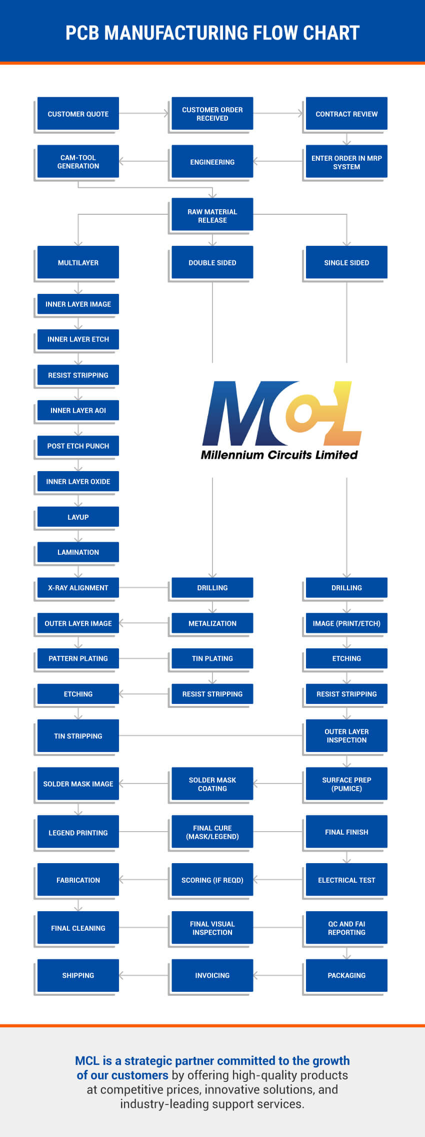
How Are PCBs Made?
The steps of the PCB design process start with design and verification and continue through the fabrication of the circuit boards. Many steps require computer guidance and machine-driven tools to ensure accuracy and prevent short circuits or incomplete circuits. The completed boards must undergo strict testing before they are packaged and delivered to customers.
Step One: PCB Design Process
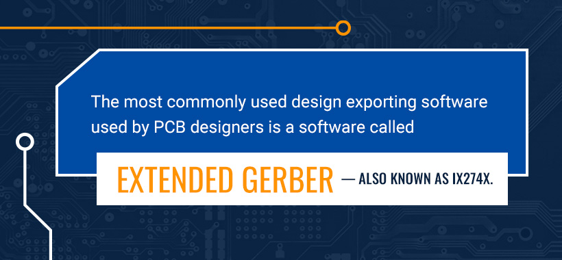
Design is the first step in circuit board manufacturing. It acts as a plan for PCB manufacture and design — the designer lays out a blueprint for the PCB that fulfills all the outlined requirements. The most commonly used design exporting software used by PCB designers is a software called Extended Gerber — also known as IX274X.
Extended Gerber is an excellent PCB design software solution as it also works in an output format. It generates all the information that the designers and PCB manufacturers need, such as the number of copper layers, the number of solder masks needed, and the other pieces of component notation. Once a design blueprint for the PCB is encoded by the Gerber Extended software, all the different parts and aspects of the design are checked over to make sure that there are no errors.
Once the examination by the designer is complete, the finished PCB design is sent off to a PCB fabrication house so that the PCB can be built. Once there, a fabricator checks the design in a process known as a Design for Manufacture (DFM) check. An effective DFM check ensures that the design is manufacturable, given the manufacturing processes’ capabilities, and will not require excess resources or time to complete.
Progressive engineers may include the PCB manufacturer in a DFM process while in the PCB design phase instead of waiting until the design is completed. This way, they can make the necessary changes before order placement, saving time and money. If critical attributes are missing from the design, it can impact the manufacturer’s ability to produce the PC board with high yields.
Step Two: Design Review and Engineering Questions
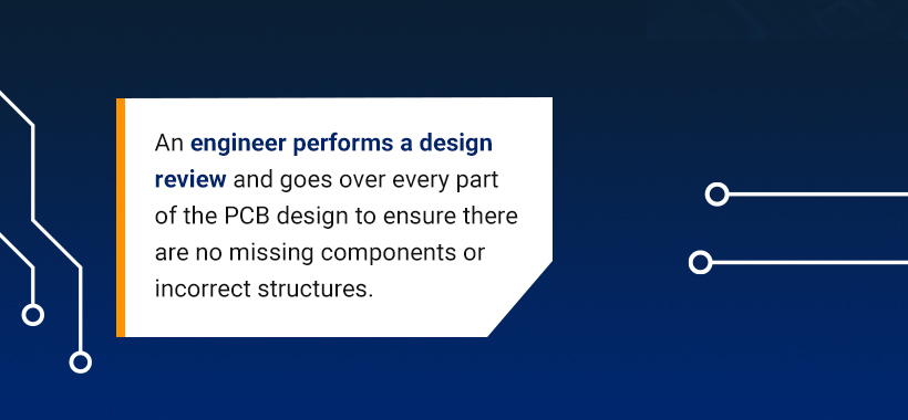
Another key step of the printed circuit board fabrication process involves checking the design for potential errors, flaws, or manufacturability issues. An engineer performs a design review and goes over every part of the PCB design to ensure there are no missing components or incorrect structures. The design moves to the printing phase after getting clearance from an engineer and the client. Clients may want to approve any working files and verify array construction, tooling holes, multi-up array orientation, scoring, and snap tabs.
Step Three: Printing
PCB plans follow a unique printing process. Unlike other plans, the process requires a specialized plotter printer to make a PCB film. Once printed, this film is essentially a photo negative of the PCB itself.
The plotter prints the PCB’s inside layers in two distinct ink colors:
- Black ink, which denotes the PCB’s circuits and copper traces
- Clear ink, which indicates the PCB’s non-conductive areas, like the fiberglass base
On the outer layers of the PCB design, this trend is reversed — clear ink refers to the line of copper pathways, but black ink also refers to areas where the copper will be removed.
Each PCB layer and the accompanying solder mask gets its own film, so a simple two-layer PCB needs four sheets — one for each layer and one each for the accompanying solder mask.
Once the films for each layer of the PCB are printed, they’re lined up, and the printers use a punch machine to punch a hole through them, known as a registration hole. This hole is an alignment guide, allowing technicians to align the films throughout the manufacturing process.
Step Four: Printing the Copper for the Interior Layers
In step four, the manufacturer begins construction of the PCB. The laminate panel is covered by a type of photo-sensitive film called the resist. The resist is made of a layer of photo-reactive chemicals that harden after they’re exposed to ultraviolet light. The resist allows technicians to get a perfect match between the photos of the blueprint and what’s printed to the photoresist.
Once the resist and the laminate are lined up — using the holes from earlier — they receive a blast of UV light.
The UV light passes through the translucent parts of the film, hardening the photoresist. This indicates areas of copper that are meant to be kept as pathways. In contrast, the black ink prevents any light from getting to the areas that aren’t meant to harden so that they can later be removed.
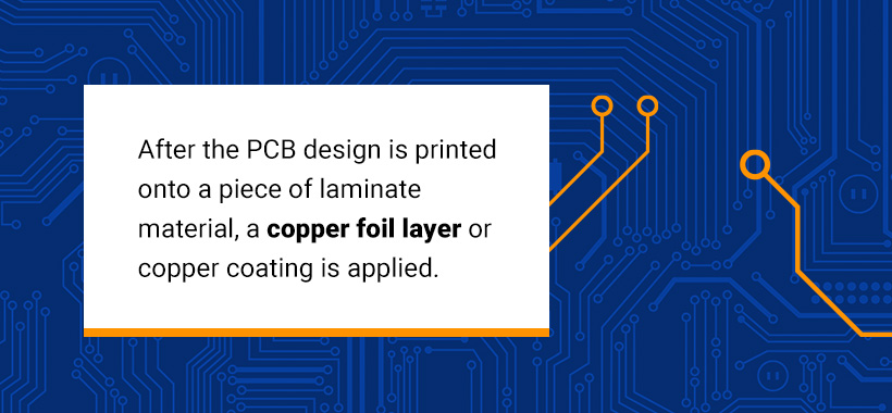
After the PCB design is printed onto a piece of laminate material, a copper foil layer or copper coating is applied. The copper is then pre-bonded to that same piece of laminate, which serves as the base for the PCB. The copper is then etched away to reveal the traces as designed on the blueprint from earlier.
The inner layers are part of a core, which has two layers of copper with dielectric material between them. The inner layers are treated with etch resist to protect the copper from etching away. The treatment is done before the core goes through the etching process. After etching, the only copper that remains is the copper intended by the designer.
Once technicians have prepared the board, they wash it with an alkaline solution or use a similar process to remove any remaining photoresists. They then pressure wash it to remove any debris or particles left on the surface and leave it to dry. Once dry, the only resist remaining on the PCB is on top of the copper. The technician then inspects the PCB for errors.
After drying, the only resist that should be left on the PCB is on top of the copper that remains as part of the PCB when it’s finally popped free. A technician looks over the PCBs to make sure that there are no errors. If no errors are present, then it’s on to the next step.
Step Five: Etch the Inner Layers or Core to Remove Copper
The core or inner layers of the printed circuit board need to have extra copper removed before the PCB fabrication process can continue. Etching involves covering the necessary copper on the board and exposing the rest of the board to a chemical. The chemical etching process removes all unprotected copper from the PCB, leaving only the board’s necessary amount.
This step may vary in its time or the amount of copper etching solvent used. Large PCBs or those with heavier structures may use more copper, resulting in more copper that must undergo etching for removal. Therefore, these boards will require extra time or solvent.
Step Six: Layer Alignment
Once technicians have cleaned each of the PCB’s layers, they’re ready for layer alignment and optical inspection. The holes from earlier are used to align the inner and outer layers. To align the layers, a technician places them on a type of punch machine known as an optical punch. The optical punch drives a pin down through the holes to line up the layers of the PCB.
Step Seven: Automated Optical Inspection
Following the optical punch, another machine performs an optical inspection to make sure there are no defects. This automated optical inspection is incredibly important because once the layers are placed together, any errors that exist can’t be corrected. To confirm that there are no defects, the AOI machine compares the PCB with the Extended Gerber design, which serves as the manufacturer’s model.
After the PCB has passed the optical inspection — that is, neither the technician nor the AOI machine found any defects — it moves onto the last couple steps of PCB manufacture and production.
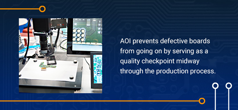
The AOI step is crucial for the operation of the printed circuit board. Without it, boards that could have short circuits, not meet the design specifications or have extra copper that was not removed during etching could pass through the rest of the process. AOI prevents defective boards from going on by serving as a quality checkpoint midway through the production process. Later, this process repeats for the outer layers after engineers finish imaging and etching them.
Step Eight: Laminating the PCB Layers
In step eight, the original piece of the substrate is also covered in a layer of thin copper foil that now contains the etchings for the copper traces. Once the outer and inner layers are ready, it’s time to push them together. A dielectric material is included between the inner core and the outer layers.
These layers are sandwiched using metal clamps on a special press table. Each layer fits onto the table using a specialized pin. The technician doing the laminating process starts by placing a layer of pre-coated epoxy resin known as pre-impregnated or prepreg — on the table’s alignment basin. From there, they construct the layers in a specific order — copper foil, dielectric, core, dielectric, and copper foil in a four-layer “book.”
Once the copper press plate is in place, the stack is ready to be pressed. The technician takes it over to a mechanical press and presses the layers down and together. As part of this process, pins are punched down through the stack of layers to ensure they’re fixed properly.
If the layers are fixed properly, the PCB stack is taken to the next press, a laminating press. The laminating press uses a pair of heated plates to apply both heat and pressure to the stack of layers. The heat from the plates melts the epoxy inside the prepreg. Alongside the pressure from the press, it combines and fuses the stack of PCB layers together.
Once the PCB layers are pressed together, there’s a little bit of unpacking that needs to be done. The technician needs to remove the top press plate and the pins from earlier, which then allows them to pull the actual PCB free.
Step Nine: Drilling
Before drilling, an X-ray machine is used to locate the drill spots. Then, registration or guiding holes are drilled so that the PCB stack can be secured before the more specific holes are drilled. When it comes time to drill these holes, a computer-guided drill is used to make the holes themselves, using the software from the Extended Gerber design as a guide.
Once the drilling is complete, any additional copper that’s leftover at the edges is filed off.
Step Ten: PCB Plating
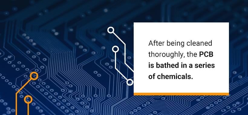
After the panel has been drilled, it’s ready to be plated. The plating process uses a chemical to fuse all of the different layers of the PCB together. After being cleaned thoroughly, the PCB is bathed in a series of chemicals. Part of this bathing process coats the panel in a micron-thick layer of copper, which is deposited over the topmost layer and into the holes that have just been drilled.
Before the holes are filled with copper, they simply serve to expose the fiberglass substrate that makes up the panel’s insides. Bathing those holes in copper covers the walls of the previously drilled holes.
The non-conductive layers have dark ink covering them, and the copper has light ink. This light ink allows for the tin plating to cover and protect the copper.
Step Eleven: Outer Layer Imaging
Earlier in the process, a photoresist was applied to the PCB panel. In step 11, it’s time to apply another layer of photoresist. However, this time, the photoresist is only applied to the outer layers since it still needs to be imaged. Once the outer layers have been coated in photoresist and imaged, they’re plated in the exact same way the interior layers of the PCB were plated in the previous step. However, while the process is the same, the outer layers get a plating of tin to help guard the copper of the outside layer.
Step Twelve: Outer Layer Etching
In the final etching stage, the temporary tin guard helps protect the copper underneath. Any unwanted copper is removed using the same copper solvent from earlier, with the tin protecting the valued copper of the etching area. After the outer layers are etched, the tin guard is removed.
One of the main differences between the inner and outer layer etching covers the areas that need removal. Engineers remove unneeded copper and any remaining resist coating during etching, preparing the outer layer for AOI and solder masking, referred to as a subtractive process.
Step Thirteen: Outer Layer AOI
As with the inner layer, the outer layers typically undergo automated optical inspection. This optical inspection ensures the layer meets the exact requirements of the design. It also verifies that the previous step removed all extra copper from the layer to create a properly functioning printed circuit board that won’t create improper electrical connections.
Step Fourteen: Solder Mask Application
Panels require a thorough cleaning before the solder mask is applied. Then, a solder mask is applied via screening or curtain costing and tack-cured. The PCB undergoes a visual inspection, which is a critical element of this setup as many original equipment manufacturers (OEMs) will not allow solder mask repairs. If there are solder mask voids or inconsistencies, the solder mask can be stripped and the process begins again.
If the solder mask passes inspection without issues, it will then be baked and cured. This mask provides the board’s copper with extra protection from damage caused by corrosion and oxidation. Next, ultraviolet light strikes the boards to indicate where to remove the solder mask. This process is referred to as the “liquid photo-imageable” solder mask application.
Step Fifteen: Silkscreen Application and Surface Finish Application
Because PCBs need to have information directly on the board, fabricators must print vital data on the surface of the board in a process referred to as silkscreen application, nomenclature, or legend printing. This information includes the following:
- Company ID numbers
- Warning labels
- Manufacturers marks or logos
- Part numbers
- Pin locators and similar marks
- Component designators, polarity marks, and connector pin-outs
After printing the above information onto the printed circuit boards, often with an inkjet printer, the PCBs have their surface finish applied. Then, they continue to the testing, cutting and inspection phases. For clarity, 8-point font and smaller silkscreen text require laser printing.
Step Sixteen: Finishing the PCB
Finishing the PCB requires plating with conductive materials, such as the following:
- Immersion silver: This plating option offers low signal loss, but the finish can oxidize and tarnish. It’s lead-free and Restriction of Hazardous Substances (RoHS) compliant.
- Hard gold: Gold is one of the more expensive plating alternatives, but it’s durable, RoHS-compliant, and lead-free. It’s often used for gold fingers for multiple insertions of daughter boards into motherboards.
- Electroless nickel immersion gold (ENIG): ENIG is one of the most common PCB finishes. It’s more expensive than other options but less than gold. It is well known for offering exceptional longevity and durability. It’s also RoHS compliant and provides better flatness and co-planarity of component pads.
- Hot air solder leveling (HASL): HASL is a cost-effective, long-lasting solution with added benefits for reworkability. However, it contains lead, and fails to meet RoHS compliance standards.
- Lead-free HASL: Removing the lead from HASL keeps its cost-effective and reworkability benefits while making it RoHS compliant. Both types of HASL are only effective with 20mm pitch devices, while 16mm pitch devices require an alternate coating for flatness and co-planarity of component pads.
- Immersion tin (ISn): This option is popular for press-fit applications, with RoHS compliance and tight hole tolerances. However, working with this medium can cause soldering problems, such as tin whiskers. It also has a short shelf-life of about 3-6 months. These PCBs must be wrapped and stored so they’re not exposed to free-flowing air, and be contained in a temperature- and humidity-controlled environment.
- Organic solderability preservative (OSP): OSP is RoHS compliant and cost-effective, but has a 6-11 month shelf life.
- Electroless nickel electroless palladium immersion gold (ENEPIG): This option requires careful processing for proper performance. It offers high solder strength and the palladium coating after the plating helps prevent nickel corrosion. However, it’s less cost-effective than options.
The correct material depends on the design specifications and the customer’s budget. However, applying such finishes creates an essential trait for the PCB. The finishes allow an assembler to mount electronic components. The metals also cover the copper to protect it from oxidation that can occur with exposure to air.
Step Seventeen: Electrical Reliability Test
After coating and, if necessary, curing, technicians perform a battery of electrical tests on the PCB. Electrical testing must adhere to the standards of IPC-9252, Guidelines and Requirements for Electrical Testing of Unpopulated Printed Boards. The main tests performed are circuit continuity and isolation tests. The circuit continuity test checks for any disconnections in the PCB, known as “opens.” The circuit isolation test checks the isolation values of the PCB’s various parts to check for any shorts.
While the electrical tests mainly exist to ensure functionality, they also work as a test of how well the initial PCB design stood up to the manufacturing process.
In addition to basic electrical reliability testing, there are other tests that can be used to determine if a PCB is functional. One of the main tests used to do this is known as the “bed of nails” test. During this text, several spring fixtures are attached to the test points on the circuit board. The spring fixtures then subject the test points on the circuit board with up to 200g of pressure to see how well the PCB stands up to high-pressure contact at its test points.
If the PCB has passed its electrical reliability testing — and any other testing the manufacturer chooses to implement — it can be moved on to the next step: route out and inspection.
Step Eighteen: Profiling and Route Out
Profiling requires fabrication engineers to identify the shape and size of the individually printed circuit boards cut from the construction board. This information typically is in the design’s Gerber files. This profiling step guides the routing out process by programming where the machine should create the scores on the construction board.
Routing out, or scoring, allows for easier separation of the boards. A router or CNC machine creates several small pieces along the edges of the board. These edges can let the board quickly break off without damage. However, some fabricators may choose to use a v-groove instead. This machine will create v-shaped cuts along the sides of the board.
PCB manufacturers will sometimes employ a hard tooled punch to separate PCBs from the manufacturing panel. However, this is typically only done in higher-volume applications. Other times, snap-tabs that are used in the design of the customer’s array allow the assembler to remove individual boards after PCB assembly.
Step Nineteen: Quality Check and Visual Inspection
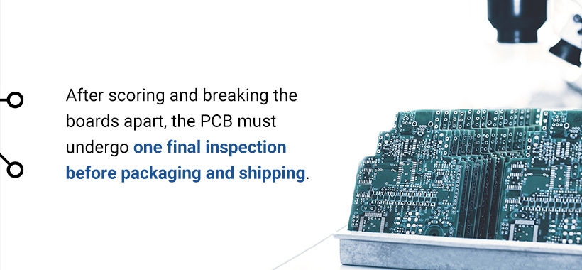
After scoring and breaking the boards apart, the PCB must undergo one final inspection before packaging and shipping. This final check verifies several aspects of the boards’ construction:
- Hole positioning and tolerances: The PCB’s hole sizes must match on all layers and meet the design requirements.
- Board dimensions: The PCB’s dimensions must align with the original design specifications.
- Cleanliness: Fabricators must ensure the boards are free from dust, debris, and unwanted particles.
- Finish: Finish boards must have smooth edges, free of burrs or sharp areas.
- Electrical reliability: Any boards that fail electrical reliability tests must return for repairs and retesting.
Step Twenty: Packaging and Delivery
The last stage of PCB manufacturing is packaging and delivery. Packaging typically involves material that seals around the printed circuit boards to keep out dust and other foreign materials, similar to vacuum packaging. The sealed boards then go into containers that protect them from damage during shipping. Lastly, they go out for delivery to the customers. Electrostatic discharge (ESD) protective packaging may be used depending on the customer’s specifications.
The PCB Manufacturing Process for Multilayer Designs
Multilayer printed circuit boards have additional steps to account for the extra copper layers and cores during their fabrication. These steps include bonding and lamination under high temperatures and pressures to eliminate air gaps. These steps keep the PCB assembly stable.
Inner Layer Imaging
Inner layer imaging follows the same procedures as printing the PCB design. The design prints on a plotter printer to create a film. The solder mask for the inner layer also prints out. After aligning both, a machine creates a registration hole in the films to help keep the films lined up properly with the layers later.
After adding copper to the laminate material for the inner layer, technicians place the printed film over the laminate and align them using the registration holes.
Ultraviolet light exposes the film, also known as the resist, to harden the chemicals of the light-colored areas into the printed pattern. These hardened areas will not wash off during the etching phase, while the non-hardened areas under dark-colored film will have their copper removed.
Inner Layer Etching
After imaging, the areas covered by clear ink have hardened. This hardened material protects the copper beneath and remains on the board after etching.
Technicians first wash off the board with an alkaline solution to remove any remaining resist from the board that didn’t harden. This cleaning exposes areas that covered non-conductive portions of the printed circuit board. Next, workers will etch off the excess copper from these non-conductive areas by submerging the board into a copper solvent to dissolve the exposed copper.
Resist Stripping
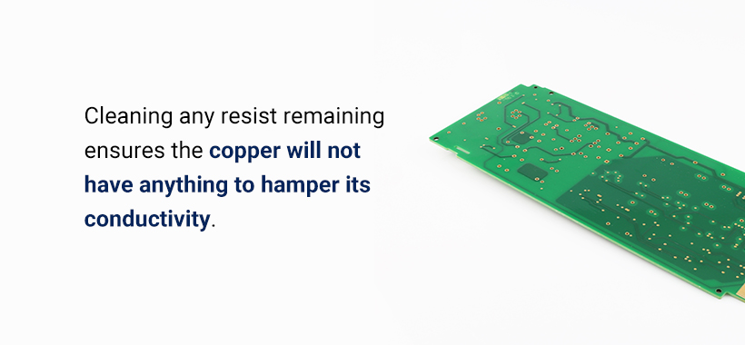
The resist stripping step removes any remaining resist covering the copper of the PCB inner layer. Cleaning any resist remaining ensures the copper will not have anything to hamper its conductivity. After removing the resist, the layer is ready to undergo inspection of its basic design.
Post Etch Punch
The post-etch punch aligns the layers and punches a hole through them using the registration holes as a guide. As with the subsequent inspection of this hole and alignment, the punching happens from a computer that exactly guides a machine known as an optical punch. After the optical punch, the layers move to the inner layer automated optical inspection (AOI).
Inner Layer AOI
Inner layer automated optical inspection uses a computer to carefully examine the inner layer to look for incomplete patterns or resist that may still be on the surface. If the PCB layer passes AOI, it moves on in the process.
Inner Layer Oxide
Oxide applied to the inner layer ensures better bonding of the copper foil and insulating epoxy resin layers between the inner and outer layers.
Layup
The layup step in the multilayer PCB fabrication process happens when a machine helps to line up, heat, and bond the layers together with a copper foil layer and insulating material between the inner and outer layers. Pins are used to secure the alignment of the various layers based on the post-etch process. They are applied before lamination to secure the layers as intended. Typically, computers guide these machines because the alignment of the layers and bonding must be exact.
Lamination
Lamination uses heat and pressure to melt the bonding epoxy between the layers. Properly laminated PCBs will hold their layers tightly together and provide effective insulation and a strong product.
X-Ray Alignment
When drilling multilayer boards after lamination, an X-ray ensures the alignment of the drill bit. These holes allow for connections to occur between layers of the multilayer PCB. Therefore, the accuracy of their placement and size in relation to the rest of the layer and the other layers is crucial. Following the layers’ X-ray alignment, the printed circuit board undergoes drilling and then picks up with the next steps for single or double-sided PCB fabrication.
How to Implement an Effective PCB Manufacturing Process
The printed circuit board manufacturing and design processes often involve different entities. In many cases, the contract manufacturer (CM) may assemble a printed circuit board with components based on the design created by the OEM. Collaboration between these groups on components, design considerations, file formats, and board materials will ensure an effective process and seamless transition between phases.
Design for Manufacturing (DFM) Considerations
Design for manufacturing considers how well the design can progress through the various stages of the fabrication process. Often, the fabricator will have a set of DFM guidelines for their facility that the OEM can consult during the design phase. The designer can request these DFM guidelines to inform their PCB designer and adapt it to the fabricator’s production process.
The designer should consult with the fabricator on available materials. Ideally, the fabricator will have all the components required by the design on hand. If something is missing, the designer and fabricator must find a compromise to ensure faster manufacturing while still meeting minimum design specifications.
File Formats
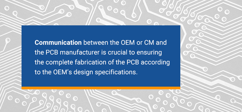
Communication between the OEM or CM and the PCB manufacturer is crucial to ensuring the complete fabrication of the PCB according to the OEM’s design specifications. Both groups must use the same file formats for the design. Doing so will prevent errors or lost information that may occur when the files must change formats.
Board Materials
OEMs may design printed circuit boards with pricier materials than the PCB manufacturer anticipates. Both parties must agree to the materials on hand and what will work best for the PCB design while remaining cost-effective for the final purchaser.
Why Trust Us?
Millennium Circuits Limited (MCL) has supplied many customers with bare printed circuit boards since 2005. We have worked with customers of various sizes across industries for almost two decades, prioritizing the customer experience and providing rapid response, flexible lead times, and technical support.
Since our inception, we have remained focused on redefining customer service and streamlining our internal practices to reflect the needs of the time. We ensure your PCBs comply with the relevant industry standards while manufacturing the highest quality products at competitive prices to benefit your bottom line.
Contact Millennium Circuits for Questions
High-quality engineering and manufacturing of PCBs are critical parts of electronic circuit board operations. Understanding the complexities of the process and why each step must occur gives you a better appreciation for the cost and effort put into each printed circuit board.
Contact us at Millennium Circuits Limited when your company needs PCBs for any job. We work to supply small and large batches of competitively priced printed circuit boards to our customers.
Summary
Key Takeaways
- PCB manufacturing is a precise, multi-step process that turns digital designs into functional boards.
- Each stage is interconnected—from imaging and etching to drilling, plating, and finishing—requiring tight process control.
- Built-in inspections and testing ensure quality and catch issues before final delivery.
- Material choices and stack-up decisions directly impact performance and reliability.
- Strong alignment between design and manufacturing improves yield, reduces errors, and speeds time to market.