Controlled Impedance
Experience flawless signal integrity with MCL’s mastery in controlled impedance. When you’re working with complex circuit boards, you’ll need to ensure that your boards provide the high performance you need. One important factor to consider is the impedance of your boards. Controlling the impedance of your boards improves their functionality.
In this guide, we’ll discuss what impedance control is and how you should specify impedance control for new PCBs. Also check out our guide for trace impedance.
What is Controlled Impedance?
Controlled impedance is a way of predetermining an electric circuit’s resistance to alternating current. That resistance arises as a function of both resistance and reactance within the circuit. Impedance is critical to a circuit’s operations because it affects the schedule on which a circuit completes its functions. It impacts the timing – and integrity – of essential processes. Controlling impedance by altering the physical structure of board components to give the impedance a particular value helps the board act as it was designed to. Controlled impedance is often a PCB design consideration for high-frequency analog circuits or high-speed digital circuits.
Impedance, generally measured in Ohms, is a characteristic of the circuit that has to be taken care of during the design of the PCB. Resistance and reactance of an electrical circuit have a major impact on functionality, as certain processes must be completed before others to ensure proper operation. This chain of command disrupts a system and leads to a complete failure when these actions aren’t performed as planned. Printed circuit boards with impedance requirements will nullify the changes in voltage occurring and lead to an appliance or gadget that operates as expected.
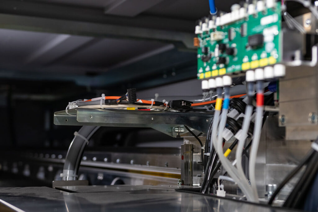
The use of differential impedance PCB components provides the control needed for a range of products. We can recommend software programs designed to detect resistance and reactance flow, providing you with the specs you require. MCL will use this data to create custom PCBs. The resulting circuitry is cost-effective and provides heightened reliability.
What Is a PCB Transmission Line?
PCB transmission lines are interconnections that move signals from a PCB’s transmitters to its receivers. Each transmission line has at least two conductors. One conductor must be a signal trace, and each transmission line must have at least one return path. Most return paths are ground planes. PCB dielectric material makes up the volume between conductors. The dielectric layer separates the signal trace from ground planes and other conductors.
Transmission lines require impedance control to solve issues with signal integrity. Controlled impedance is key to propagating signals in waves, without distortion, when high-frequency signals travel over PCB transmission lines. If impedance varies between transmitters, a signal reflection occurs. The reflected signal superimposes itself on the original signal, distorting it.
Often, a distorted signal cannot perform its intended function. Implementing a uniform controlled impedance at each point minimizes signal distortions. Impedance control basics improve signal integrity.
The PCB’s physical dimensions and the materials within its dielectric layer determine the impedance of a circuit, which is measured in Ohms.

What Are the Types of PCB Transmission Lines?
Stripline and microstrip lines route high-speed transmission lines over a printed circuit board. Most PCB manufacturers use either stripline or microstrip, though a third option also exists. Co-planar waveguide transmission lines are the third option, but they’re far less common.
Each type of transmission line has its own benefits. Various designs have individual needs that make one type or the other more suited for the PCB’s applications. Many dense, high-speed PCBs have multi-layer boards. These configurations feature both stripline and microstrip lines.
Stripline
A PCB with a stripline has a uniform trace for the signal on the circuit board’s inner layer. A parallel PCB dielectric layer separates the trace from the conducting planes on either side. Each of the two conducting planes acts as a return path.
The second ground plane allows for thin, controlled impedance traces. Smaller trace widths increase density, so stripline transmission lines are compatible with more compact designs. Stripline’s internal layer offers hazard protection and reduces electromagnetic interference (EMI).
Microstrip Line
Unlike a stripline’s embedded trace, the single uniform trace on a microstrip line is located on the outer layer of a PCB. The trace is parallel to the return path of the ground plane conductor. PCB dielectric separates the trace from the ground planes. Microstrip line’s simple layer structure lowers production costs.
Pairs of microstrip lines with balanced signals are differential microstrip lines, which can carry high-speed signals.
PCB Transmission Lines That Require Controlled Impedance
Beyond the distinction between stripline and microstrip line, other differences separate various transmission lines. Embedding the exposed trace of a microstrip line in the dielectric layer, for example, creates an embedded microstrip. Another common alteration is coupling PCB transmission lines into differential pairs.
A differential pair is a balanced pair of conductors, like transmission lines. These pairs transfer energy and are subject to impedance. Each of the following PCB transmission lines requires controlled impedance:
- Single-ended microstrip
- Differential pairs of microstrip
- Embedded microstrip
- Single-ended stripline
- Differential pairs of stripline
- Single-ended co-planar waveguides
- Differential pairs of co-planar waveguides
Factors That Affect Impedance Control During PCB Design
A few factors that affect impedance control during PCB design include trace width, copper thickness, dielectric thickness and dielectric constant. Below is a breakdown of what effects these factors have:
- Trace width: On a PCB, the trace width is the width of the copper foil, plus its coating. As trace width increases, impedance tends to fall. When designers create the specifications for PCBs, they base trace width on a few different factors, including capacity and temperature rise. If they have a particular impedance in mind, they can design for that as well.
- Copper thickness: The thickness of the copper on the PCB affects impedance as well. As with the trace width, as copper thickness rises, impedance tends to fall. If designers want to decrease impedance, they can increase copper weight and thickness. On the other hand, if they want to allow higher impedance, they can reduce copper weight and thickness.
- Dielectric thickness: Dielectric thickness is the thickness of the insulating material between traces. Dielectric thickness and impedance have a logarithmic relationship — large increases in thickness tend to produce more modest increases in impedance. To reduce impedance, designers can substantially reduce the thickness of the insulating material.
- Dielectric constant: The dielectric constant is the ratio of the electric permittivity of a material to the electric permittivity found in a vacuum. In a PCB, dielectric constant tends to vary inversely with frequency. A PCB with a low, stable dielectric constant is suitable for high frequencies and controlled impedance. A more difficult dielectric constant can often affect impedance in unpredictable ways.
When Is Impedance Most Important?
Operations controlled by impedance printed circuit boards perform faster processing and use less energy. Covering impedance control in PCB design plans helps products perform better for longer periods of time, improving value and controlled reliability.
Controlled impedance is essential during transitions from a lower Ohm to a higher Ohm environment where impedance is present. These kinds of transitions can lead to energy reflection in the form of powerful pulses capable of disrupting energy flow. This issue is as critical for those manufacturing high-powered digital devices as it is in radio frequency (RF) applications.
At MCL, we also manage electromagnetic interference (ELI) through the use of specially designed PCBs with impedance requirements built-in during manufacturing. A pulse of reflection energy disrupts circuits. That distortion often bleeds over to neighboring components. It interrupts energy flow and leads to product operation failures.
How Does PCB Impedance Control Work?
Before you can decide what kind of impedance control service you need for your printed circuit boards, you need to understand impedance control basics. What is impedance control, exactly, and how does it work? There are three basic levels of service when it comes to PCB impedance control:
- No impedance control: This is a situation where you do not need any extra design elements to ensure correct impedance because you have very loose impedance tolerance. Naturally, this will result in a faster-completed, less expensive board because the manufacturer does not have to include any special measures.
- Impedance watching: What is impedance watching? This is a situation where the designer will outline the impedance control trace, and the PCB provider adjusts the trace width and dielectric height accordingly. Once the manufacturer approves these specifications, they can begin to manufacture the board. You can request a time-domain reflectometry (TDR) test to confirm the impedance for a fee.
- Impedance control: Actual impedance control is something you will typically only request when your design has tight impedance tolerances that could be tough to hit the first time around. When the capability limits of the manufacturer get close to the dimension requirements, it can be tough to ensure target impedance on the initial attempt.
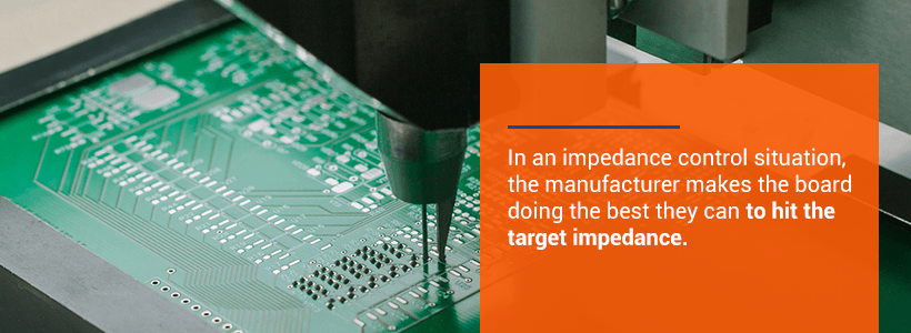
In an impedance control situation, the manufacturer makes the board doing the best they can to hit the target impedance. They then run a TDR test to see if they are successful. If not, they adjust accordingly and try again until they achieve the desired impedance.
What Is Impedance Control on a Microstrip?
There are four parameters to consider when it comes to impedance for a microstrip:
- Dielectric height, or H, which you can adjust incrementally (e.g., +1mil =+2 Ohms)
- Material dielectric, or Er, which will be fixed once you choose your material
- Trace thickness, or T
- Trace width, or W
Standard final impedance tolerance is about +/- 10 percent.
How to Specify PCB Impedance Control
In the documentation materials they create to send to fabricators, designers already typically include callouts for different specifications, including material types, copper weight and the number of layers. Therefore, it’s easy to provide additional specifications for impedance as well.
To specify impedance, designers typically need to specify values for a few different parameters:
- Target impedance
- Trace width
- Trace height
- Layer or Layers the impedance trace or traces are on
- Spacing between copper components on controlled traces (for coplanar or differential calculations)
If your requirements are extremely particular, you might consider including a chart that lays out impedance targets, trace widths, copper weights and layer thicknesses. Adding a chart can help clear up confusion by providing a visual representation of the provided specs.
These are only a few parameters, and some of this information may already be included in the PCB documentation. So, in some cases, the extra work necessary to specify impedance control is minimal.
If designers fail to specify impedance control by leaving these parameters out of the documentation, delays may occur. For instance, a fabricator may not be sure whether vague specifications call for impedance control in all layers of a multilayer board or in only some of the layers — or the documentation given may provide many details for specifications with impedance controls like copper weight and layer thickness but fail to specify what trace width needs to be controlled.
In any situation like this, the fabricator may have to go back to the design team with questions. Extremely complex boards or wildly incomplete specifications may give rise to several rounds of queries before the fabricator is satisfied that work can proceed. These rounds of questioning take up valuable time. To make sure projects proceed efficiently, it’s essential to specify impedance control correctly and with the necessary detail.
Get a Free Quick Quote.

Common Impedance Mistakes to Avoid
When you’re specifying impedance control, particularly with multilayer PCBs, you’ll need to minimize errors to ensure the timeliness and quality of your project. Below are a few common impedance mistakes to watch out for:
- Trace width inconsistencies: Remember that only one trace width is possible per PCB layer. If your specifications call for a .004-inch and .008-inch trace for the same board layer and the same impedance, your fabricator will have to stop production and ask you which figure to use.
- Failing to specify layers: Some of your specifications may apply only to specific layers of your PCB — but if you don’t indicate which ones, your fabricator may assume they apply to all layers. If you have a dense board — say a board with twenty layers or more — the confusion can lead to extensive, unnecessary work and significant delays.
- Unreasonable impedance targets: Most impedance tolerances fall into the range of about +/- 10%. If you ask for a much tighter impedance tolerance, the fabricator may assume it’s an error and stop work to ask you for clarification. Tight tolerances are often significantly more expensive because even small nonconformities that would otherwise be permissible can result in extensive reworking. So, be sure you’ve specified the correct range.
- Notes and stackup inconsistencies: Be sure that all the information you submit with your documentation matches. If the stackup image in your CAD design contradicts the specifications written in your notes, delays will likely occur until you can provide clarification. It also sometimes happens that the CAD drawing includes a standard stackup image instead of a stackup that matches your design — inconsistencies like these can also lead to delays.
Here’s How We Do It
At Millennium Circuits, we’ve developed a tested and reliable method for controlling impedance as we create a circuit. Here’s how it works:
- You let us know what specifications you require for your boards.
- We put the different elements of the PCB in place.
- We change the flow of energy by altering the physical characteristics of the PCB. We adjust elements like the thickness of the copper and the physical relationships between components to give your boards the impedance you’ve requested.

Contact Millennium Circuits for More Information About Controlled Impedance
To see the benefits of PCB impedance testing and control, make Millennium Circuits your trusted partner for PCB engineering solutions.

Provide us with the specs you need, and MCL will create the most robust circuitry available with all the benefits of flexible applications using our state-of-the-art systems. PCBs are more cost-effective and easier to use, and they allow for greater numbers of circuits to be utilized in small spaces. Take advantage of these benefits while retaining the ability to fine-tune your processing times. Get in touch with MCL today to discuss our controlled impedance capabilities.
Contact us today to learn more.