
Updated on December 3, 2024
PCB Failure Analysis and Common Issues
Printed circuit boards (PCBs) are critical components for a variety of industries and devices, including medical equipment, satellites, wearables, and airplanes. Over the past few years demand for these devices has grown even higher, and experts anticipate the global industry to grow to $78.2 billion by the end of 2024.
With the sheer amount of money and industries supporting these devices, it’s easy to see the importance of functioning PCBs. However, like every other type of equipment, PCBs can face several unique issues that impact operation. Troubleshooting printed circuit boards is crucial for addressing repair concerns and ensuring teams have the tools they need to support tasks.
Learn how to troubleshoot a PCB by discovering the common reasons for failure and how to address them.
Table of Contents:
- Why Do PCBs Fail?
- How to Tell if a Circuit Board Is Bad
- Reducing PCB Design Issues
- Troubleshooting PCB Problems to Prevent Failure
Why Do PCBs Fail?
PCB damage can vary in severity, with the end result potentially leading to complete failure. The manufacturing and design process of PCBs is complex, requiring precision, accuracy, and great attention to detail. Design oversights like incorrect dimensions or insufficient clearances can impact a PCB’s function. PCB manufacturing defects like over-etching or drilling errors can also cause defects.
The function of these devices can also leave room for error. PCBs connect various components through complex circuitry, meaning there are also several opportunities for problems to occur as teams use a PCB for daily operations.
Regardless of the reason for failure, it’s crucial to address these issues promptly, taking the right actions to ensure PCB integrity for future production runs. Fortunately, understanding the manufacturing process and becoming aware of common PCB issues can help you avoid device problems.
How to Tell if a Circuit Board Is Bad
Troubleshooting electronic circuit boards starts with determining whether you have a faulty PCB and what issues it possesses. PCB failure reasons range from minor pain points to significant issues. Common PCB defects often fall within one of these four categories:
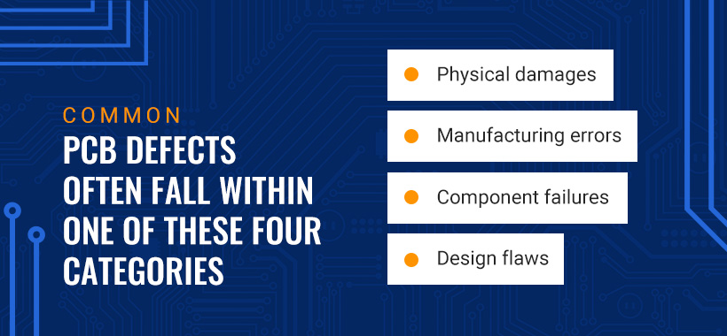
- Physical damages: PCBs are fragile devices that can face significant damage from water exposure, dust buildup, drops, oxidation, vibration, or heat damage. Obvious signs of wear and tear, such as corrosion, often indicate when you have physical damage.
- Manufacturing errors: Small oversights in manufacturing can have significant impacts on PCB function. Sometimes, manufacturers can catch these problems late in the process, while other times, a problem may go unseen until an operator puts it to use.
- Component failures: Like most devices, PCBs rely on a variety of components, and over time, these components wear down. As components age, they may malfunction or stop working altogether. Some parts are prone to failure sooner than others, so it’s important to understand your components.
- Design flaws: Human error can also cause PCB design flaws. Actions such as incorrect component placement or improper material selection can reduce performance efficiency and lead to premature failures.
This list is not exhaustive, and there are many different problems that can occur with these categories. Take a look at the signs of PCB failure and common issues below:
1. PCB Assembly Issues
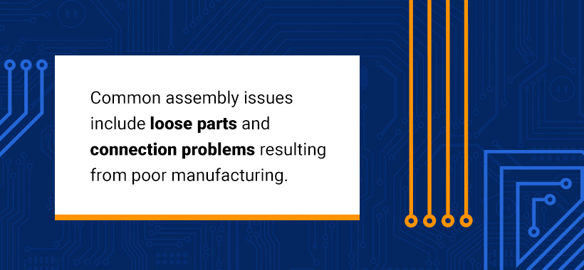
Poorly manufactured components or inadequate materials can cause PCB quality issues. When engineering teams use damaged or improper components during assembly, the PCB can face harm and experience component failure. Common assembly issues include loose parts and connection problems resulting from poor manufacturing.
Another element to watch out for is residual flux. Residual flux is a substance that teams often use during the soldering process. This substance ensures solder bonds correctly to the pads or pins, making it an essential piece of the process. However, leaving residual flux on a PCB can cause significant damage. Flux residue can lead to poor connections, react with an applied voltage to cause electrical current leakage, and pull moisture into the board, causing corrosion.
2. Plating Voids
Plated through-holes are conductor-coated holes in a printed circuit board. In many cases, the conductor will be copper, but there are other options. These holes allow electricity to be carried from one side of the circuit board to the other. To create these holes, the PCB fabricator drills holes through the circuit board, puncturing the base material all the way through. A layer of copper foil or a copper coating is then added to the surface of the material and along the walls of these holes through an electroplating process. This process deposits a thin layer of electroless copper onto the circuit board in a process called deposition. After this step, extra layers of copper are added and etched to create the trace image.
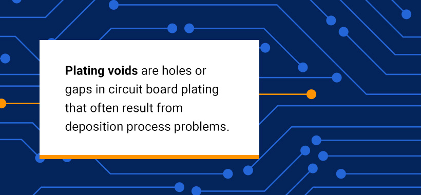
Although this process is effective, it can sometimes result in plating voids. Plating voids are holes or gaps in circuit board plating that often result from deposition process problems. These voids can cause significant issues because plating imperfections in through-hole boards can prevent electrical currents from passing, resulting in defects.
Often, this issue occurs when the deposition process results in uneven material coats. Air bubbles, material contamination, insufficient hole cleaning, and poor catalyzation of the copper in the deposition process can cause plating voids along the trace hole walls. You can often avoid defects from insufficient cleaning, air bubbles, or contamination by cleaning the material properly after drilling. Additionally, closely following manufacturer directions during use can help avoid defects from faulty drilling. For instance, following guidelines regarding drill speeds, drill in-feeds, and number of drill hits can help avoid this problem.
3. PCB Acid Traps
An acid trap refers to a circuit’s acute angles. Acute angles are capable of trapping acid during etching processes, allowing the acid to build in the angle’s nook. These small angles keep the acid in the corners for prolonged periods much longer than the design calls for. This prolonged exposure allows the acid to eat away at the material, which can result in compromised connections that make the trace defective.
Although most designers are aware of this issue and attempt to avoid it, small mistakes can lead to inevitable problems. Typically, human error will be the cause of acid traps, but some design software programs may set traces to acute angles if teams do not adjust the settings properly. Drilling extra vias or leaving gaps between vias can help prevent them from forming acid trap pockets.
4. Thermal Issues in PCB
Thermals connect pads to the plane. These small traces surrounding pads allow the pads to disperse heat more effectively, making them important pieces during the soldering process. However, sometimes, the voids between the thermal and the plane, pin or pad can cause incomplete connections, creating starved thermals, which reduce heat transfer system effectiveness. The result is several functional problems.
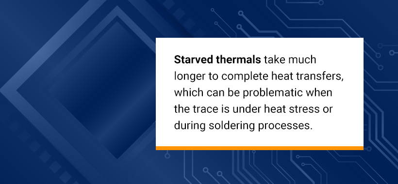
Starved thermals take much longer to complete heat transfers, which can be problematic when the trace is under heat stress or during soldering processes. Thermal pads with improper heat transfer might solder oddly and take prolonged periods to reflow, which slows the assembly process. It also exposes the component to a higher level of heat, sometimes above design limits, that would otherwise be experienced, potentially damaging the component. Circuit boards with starved thermals can suffer from insufficient heat after the manufacturing process and become prone to overheating and heat damage.
Generally, replacing the thermal is the best way to overcome this problem. However, you can also attempt to spread heat as much as possible. For instance, heat sinks and fans can transfer heat from the PCB, reducing damage. Keep in mind that small devices may not be compatible with these installs, so using a thicker copper for a higher current may address the problem.
5. Insufficient Copper-to-Edge Clearance
Copper is an incredibly conductive metal, which is commonly used as a conductive element of PCBs. However, copper is also relatively soft and vulnerable to corrosion. To prevent corrosion and protect the copper from interacting with its environment, you can cover copper with other materials. However, when trimming a PCB, if the copper is too close to the edge, part of this coating can be trimmed as well, exposing the copper layer underneath. You can also cause the protective material to delaminate from the PCB and allow intrusion, even if it is not exposed. This can cause numerous problems in the functionality of the board.
For one, it is possible for the exposed copper planes to make contact with one another by simultaneously touching a conductive material, causing a short. This exposure also leaves the copper open to the environment, making it vulnerable to corrosion and contamination if the environment has conductive, foreign objects. In addition, poorly insulated copper tracks are more prone to plating voids.
You can easily avoid this problem by making sure the space between the edge of the copper and the edge of the board, also known as the copper-to-edge or plate-to-edge clearance, follows acceptable standards for the type of board being manufactured. A thorough Design for Manufacturability (DFM) check by your manufacturer will usually catch any potential problems.
6. Bow and Twist Issues
Bow and twist deformation in PCBs can result from factors like composite PCB construction, plating stresses, uneven support and tooling, thermal metal deposition, and more. Essentially, these elements create additional stress in the PCB, leading to deformities.
The bow and twist issue on printed circuit boards can cause components and parts to shift in the PCB assembly process. If the surface mount and through-hole components x/y and z coordinate do not match the PCB, then the PCB assembly process can become very time-consuming and difficult.
You can do several things to prevent bow and twist in PCBs. First, PCB designers can balance the design by using copper thieving. This strategy helps distribute the copper evenly, preventing deformations. You can also bake PCB to eliminate moisture and ensure flat surface placement during cooling. Watch thin boards very carefully during each stage of the process, as these PCBs are more prone to warping or twisting.
It is important to note that adding thermal loads can cause these issues. PCBs are composites, meaning they are comprised of many different materials. Each material contracts and expands at a different rate. If a component expands faster than the surrounding material, it will cause stress in the material. The only way to relieve some of this stress is for the whole system to warp or move to the lowest energy position to accommodate the expanding or contracting material.
7. PCB Soldering Defects
Improper soldering during the printed circuit board assembly process can lead to major issues. One of the most common problems is cold soldering, which is when a technician doesn’t heat the part enough — this can cause PCB failure. Additionally, moisture during the soldering process can contaminate the PCB pad and other components. This contamination can cause PCB components to burn and create connection problems.
Several other issues can result from soldering defects, including black pad and solder mask outgassing. Black pad refers to an inferior connection that occurs between the solder and nickel interface. Many professionals consider this phenomenon to be extremely rare — occurring by some estimates in less than one or two percent of electroless nickel immersion gold (ENIG) PCBs. However, the fact that teams do not discover a black pad problem until an assembly process commences makes it a costly error to discover and correct in the post-manufacture phase.
Outgassing is an indicator that material is releasing a form of gas in a given environment. Although this gas can sometimes be air, it is often some sort of volatile compound that is given off by the material itself. In some cases, heating a material can cause substance breakdowns, releasing atomic gas particles.
Typically, outgassing results from wave or hand soldering during production or applications leveraging ultra-high vacuum environments that cause vapors to escape the PCB and condense or even bond with nearby surfaces, including itself and other equipment. Incorrect materials and faulty manufacturing are the top causes of outgassing. This issue can lead to other problems, such as creating voids between the copper plating and contaminating sterile environments.
Companies often use visual or X-ray inspections to detect bad soldering. However, there are other ways to address the specific issues of black pad or solder mask outgassing. To prevent black pad, it is essential to monitor and control levels of phosphorus during manufacturing. To reduce outgassing in ultra-high vacuum environments and contamination in sensitive or sterile environments, proper material selection is crucial for suiting applications. Teams can also reduce the likelihood of these issues by baking PCBs during production to reduce moisture and implementing vents or directing the board away from critical equipment to prevent contamination.
8. Pad Lifting
The pads on your printed circuit board are there so component pins can make connections to the copper plate. However, if you have lifted pads, the pins may not be able to make that connection cleanly, and the component will fail. Pad lifting is most common on single-sided boards, but it is possible for pad lifting to occur in plated-through hole boards. In most cases, lifting will occur when heating the board’s surface causes the copper adhesion to lower. However, a combination of serious physical padding and extreme heat can also cause pad lifting.
Although there is little you can do to control thermal elements that impact pad lifting, you do have some control over some mechanical aspects. For example, you can prevent pad lifting by removing single-sided boards from the conveyor belt or pallets very carefully and instructing your team to not use large components as handles.
If you encounter pad lifting, you can try a few strategies to address the issue. Try these steps:
- Find where the trace the pad lifted from starts and ends, then run wires to every disconnected point. For the lifted pad, stick the component through the hole and solder your wire to the component leg.
- Glue the pad back to the circuit board with a strong epoxy.
- Bend the component lead to replace the track where the solder pad/trace that lifted should be and solder it directly to the track that still has a connection to the board.
- If the lead is too short, solder an extension onto the lead, then proceed.
9. Conductive Anodic Filament Formation
A growing concern in the electronics industry is conductive anodic filament (CAF) failure. CAF failure occurs when the conductive material grows from the anode to the cathode, causing an electrical failure. CAF failure is generally a two-stage process, with the first stage allowing you to reverse degradation but the second phase causing irreversible damage.
There are several ways to prevent CAF failure. Consider these factors that impact CAF failure to determine how you can reduce adverse outcomes:
- Moisture and humidity: Higher water content increases the likelihood of CAF failure because it requires an electrolyte. This means that higher humidity levels translate to higher moisture content and decrease CAF performance.
- Acid contamination processes: Some fabrication processes can introduce acid contamination, which enhances CAF formation likelihood. Examples include using some types of soldering fluxes and introducing acid residues during plating processes.
- Bias and voltage: Bias voltage is the force that drives the CAF formation reaction. Low-voltage bias can significantly decrease CAF formation, and lower voltages lower CAF likelihood as well.
- Preexisting defects: Defects like contamination, voids, wicking, fracturing, and misregistration can create filament pathways. Even partial defects like incomplete feature bridging can lead to this issue. Additionally, high temperatures, reflow, and repetitive thermal cycling can place more stress on the PCBs, increasing the chances of CAF formation.
- Materials: PCB quality issues surrounding materials can also impact CAF failure. Materials that are CAF-resistant can prevent formation, effectively addressing the issue before it occurs. Using a combination of resin systems and glass finishes can prevent CAF formation, and additional precautions can help preserve glass-resin bonds.
- Design: Small gaps between voltage failure features, the size of drilled holes, copper thickness in plated-through holes and, line-to-line spacing impact CAF resistance. In truth, many elements of the design process affect the likelihood of CAF formation, including layout, bias voltage, voltage levels, materials, and more, highlighting the importance of a quality production process.
10. Interconnect Defects
During PCB production, manufacturers often drill precise holes through multi layer PCBs to expose traces. These traces are connected by the addition of conductive material to connect all of the exposed circuitry.
However, sometimes, a defect occurs in or near this drilled hole. This flaw is called an interconnect defect (ICD) or inner-layer separation. As the term implies, ICDs involve a separation between the copper filler and the circuits. These components must connect properly for the PCB to function correctly. Inner-layer copper reliability is key to creating a functional PCB that doesn’t damage your system.
An ICD most often happens in response to thermal shocks like soldering. You usually find an ICD on the first inner layer on both sides of the board and much less frequently on deeper layers. Generally, there are two main causes of ICDs:
- Debris-based: Debris, drill smear, and inorganic filters or glass particles can enter the interconnection hole during the drilling process. Although cleaning these substances from the PCB is a standard step in the manufacturing process, sometimes teams overlook this step or don’t complete it properly. In most cases, debris causes ICDs in low-loss materials featuring inorganic filters.
- Copper bond failure: If an ICD does not come from debris, it likely originates from copper bond failure. Sometimes, the inner copper layer can break or fail to connect when the bond undergoes high stress. Larger holes and thicker PCBs are more likely to experience copper bond failure ICDs as bonds may be weaker or insufficient.
To prevent PCB separation, teams should test for this problem before allowing the board to move forward in production. However, ICDs may not appear during tests because they respond to stress, meaning they may appear in usage or assembly. These reasons make it imperative to take a proactive approach to preventing ICDs. Manufacturers can best reduce the risk of ICDs by desmearing drill hole walls, using materials with high-temperature resistance, and ensuring electroless copper has the proper grain structure and thickness to withstand stresses.
11. Electromagnetic Issues
Electromagnetic compatibility and electromagnetic interference are two problematic areas for circuit board designs. Electromagnetic compatibility (EMC) involves the generation, propagation, and reception of electromagnetic energy, while electromagnetic interference (EMI) refers to the unwanted and damaging effects of this EMC. Too much EMI can result in a defective product. Normally, these issues are a result of one of many possible design flaws.
Specific elements to consider include:
- Ground plane: Designing a PCB’s ground plane is crucial for reducing EMI. All traces need a ground to work, and this element protects against EMI. To optimize the ground plane, follow best practices like using solid planes, maximizing ground area, connecting bypass or decoupling capacitors, minimizing signal length, and using split planes carefully.
- Trace layout: Traces are also critical for board design. These conductive paths contain electrons that flow when the trace is active. Simple bends or crosses can interfere with PCB electromagnetic functions. Proper trace usage ensures properly propagated current. However, many problems can arise if teams do not arrange traces according to EMC design rules. Some practices to keep in mind for trace layout include avoiding right angles, shortening return paths, keeping signals separate, and using vias carefully.
- Component arrangement: Electronic components are the building blocks of an electronic trace. However, arranging them improperly can cause several EMI issues. When designing a PCB, be mindful of each piece’s EMI impact. Some best practices for component layout in PCB design include separating analog and digital parts, separating analog and high-speed pieces, and considering the need for high-speed components.
- EMI shielding: Some components will produce EMI no matter what design rules you follow — especially small, high-speed parts. Fortunately, shielding and filtering can keep this EMI’s effects to a minimum. Some options include low-pass filtering, component and board shielding, and cable shielding.
You can reduce EMI by increasing the circuit board’s ground area and compartmentalizing the board specifically for EMI. Additionally, 90-degree angles should be avoided for most components because they tend to increase EMI interference. When in doubt, use shielded cables during cable assembly and metallic packaging to absorb EMC and reduce EMI.
A PCB manufacturing expert can aid in circuit board troubleshooting and identify these potential design flaws and work with you on a redesign if EMC and EMI are noted as problems during the prototyping stage. If you are having EMI issues between multiple boards in the field, it may be beneficial to encase each one in a grounded conductive box.
Another major issue when it comes to high-speed PCB layout guidelines and EMI is signal integrity. Loss of signal integrity with PCB units has long been an ongoing concern, so it’s important to keep signal integrity PCB layout considerations in mind when manufacturing, selling, or purchasing printed circuit boards.
Several factors impact signal integrity — frequency and length. Low frequencies often do not omit significant signal integrity problems. However, as you increase signal frequency, it can potentially impact the systems’ analog and digital properties. This change can result in ground bounce, reflections, crosstalk, and ringing, which can damage your signal integrity. The length of the transmission medium is also essential to consider. Longer transmission mediums present a greater chance of signal loss.
Thankfully, you can often combat other signal integrity issues by adhering to best practices in design and being mindful of basic layout guidelines. Avoiding right angles, using vias sparingly, and keeping high and low speeds away from each other are simple best practices that can help you avoid signal integrity issues.
12. PCB Ionic Contamination
Ionic contamination happens when ionic residues that interfere with reliability and functionality remain on a complete PCB. An ionic residue contains atoms or molecules that become conductive when in a solution. Moisture and water exposure makes ionic residues dissociate into charged elements, which typically increase the solution’s conductivity. Several ionic residues can impact PCBs during production, including:
- Flux activators
- Salts
- Plating chemicals
- Flux activators
- Perspiration
- Organic and inorganic acids
Ionic contamination often comes from one of two sources — a lack of bare board cleanliness or through the use of aggressive chemistry. Board cleanliness impacts ionic contamination because many contaminants come from the board itself. Residues from dust, salts, oils, and environmental elements can contaminate the board, leaving it susceptible to this problem. Aggressive chemistry can also cause ionic contamination because some substances and compounds can leave behind residues that alter the board’s conductivity without proper cleaning. Either way, this issue can cause problems such as corrosion, electrochemical migration, and dendritic growth.
To avoid the adverse effects of ionic contamination, teams should conduct cleanliness testing. Methods for ensuring proper cleanliness include administering an ion chromatography test, resistivity of solvent extract (ROSE), modified ROSE test, and resistivity testing in batch-format aqueous cleaning systems.
13. Measling and Delamination
Another cause of damage to PCB components is measling and delamination. Circular white spots and small hole-like areas that appear in your printed circuit boards are typically measling and delamination errors that can occur during the production or use of PCBs. These errors can interfere with normal operations and may ruin your PCB.
While measling and delamination may appear similar, there are some noteworthy differences to keep in mind.
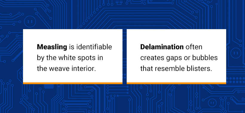
Measling is identifiable by the white spots in the weave interior. These components signal element destruction. While your board can tolerate minor measling, frequent measling or bridging measling connecting conductors and soldering eyes can be a significant issue. Most often, production and stress product measling.
Delamination often creates gaps or bubbles that resemble blisters. This occurs when PCB base materials undergo partial separations. The production process often causes delamination if too much humidity or heat is present. However, delamination can also be caused by drops and other sudden force events, mechanically forcing the layers apart.
To prevent measling and delamination, teams must manage the manufacturing process to ensure proper resin controls and temperature. You can also reduce these occurrences by storing circuit boards in dry spaces, baking the boards before thermal processing, and ensuring inner oxide layer quality.
14. Environmental-Related Issues
Various environmental factors can also impact PCBs. These devices are beneficial for a variety of industries, which means they face many unique environments. In the most basic uses, PCBs often face dust, heat, cold temperatures, and moisture, each of which can cause failures. For example, dust can clog the board, leading to overheating and weakened connections. Excess moisture can lead to oxidation, corrosion, and rust. Temperature changes can also impact your board by warping or damaging the soldering joints if elements contract or expand.
Creating a suitable environment in a dry space and implementing proper care measures can help you combat environmental-related issues. Additionally, you should opt for protective coatings and boards using resistant materials that are relevant to your line of work.
Reducing PCB Design Issues
PCB troubleshooting takes time, but mistakes in your printed circuit board design can lead to increased costs for your engineers, designers, and manufacturers while slowing your time to get to market. That hurts your revenue and can lead to significant problems in your department.
No one wants to experience those concerns, so we’ve put together this quick look at some ways to reduce PCB design errors. We’re addressing the most common concerns, but remember to always work with an engineering team whose focus is to limit PCB design errors in the production phase.
Take a look at how you can reduce bare PCB defects and design issues:
- Look for component concerns: Component placement is a significant aspect of PCB design. You must ensure each component can function and support all operational needs without interfering with other components. Keep general placement guidelines in mind, and leverage other best practices to ensure integrity. For example, matching proper voltage drops for high-current connections, utilizing ground planes or power planes for heat flow, setting vias near layer transitions, and shielding sensitive components can ensure suitable design and board longevity.
- Check thermal considerations: Smart thermal designs ensure your board can maintain proper temperatures and can simplify heat management processes. Teams should check heat against copper thickness and manage layers to ensure the continuity of thermal paths. Introducing solid ground layers and power planes can also help you reduce heat.
- Get your files together: Delivering the right files to your manufacturer can help reduce design errors and make the manufacturing process easier. Notations, component maps, drill files, tool lists, top and bottom definitions, FAB outlines, and aperture lists for older file formats are some of the essentials you should gather.
- Understand manufacturing changes: You can often find ways to save on costs while reducing design errors for your PCBs. Utilizing best practices helps you achieve savings through proper component and spacing and reducing threats. Connecting with your manufacturer about cost structure for special requirements and seeing if they can assist in engineering processes can allow you to face fewer problems and limit production errors, translating to savings in time and money.

Troubleshooting PCB Problems to Prevent Failure With MCL
PCBs are critical for operations across various industries, so understanding the common issues they face and how to prevent them is critical for ensuring smooth operations. Effective printed circuit board troubleshooting also involves finding a well-qualified and experienced PCB manufacturer to avoid issues from occurring in the first place.
At Millennium Circuits Limited (MCL), you can find the knowledgeable and dedicated team you need to solve PCB issues and identify any needs for alterations. Our team has been working on PCBs since 2005, giving us a comprehensive knowledge base and plenty of experience addressing a variety of needs.
The experienced engineering team at MCL can run complete checks on your PCBs, store information, and communicate results to keep you in the loop. Whatever kind of PCB support you need, we’ve got you covered. We proudly serve customers in various industries, including radio-frequency, LEDs, power electronics, contract manufacturing, high-speed digital, semiconductors, and instrumentation.
Contact us with any questions or to speak with MCL’s award-winning support team!