Jump To:
What Is Design for Manufacturing?
What’s the Purpose of DFM?
The DFM Factors
How Design for Manufacturing Translates Into PCB Layout
DFM Checks From Millennium Circuits Limited
Design for Manufacturing PCBs
Throughout the manufacturing and business sectors, a vast number of machines rely on printed circuit boards, or PCBs. Likewise, the capabilities of PCBs make the devices consumers use daily a reality.
With so much at stake in the design and manufacturing of PCBs, it is crucial to implement production with maximum efficiency. For this to happen, however, all the parties involved in the design stage and manufacturing process must be in constant contact to see a product idea to its fruition. Here is where the concept known as design for manufacturing and its sequence of steps come into play.
What Is Design for Manufacturing?
Design for manufacturing (DFM) is a process that enables manufacturers to examine the design of a product in a series of categories to optimize its dimensions, materials, tolerances and functionality through the most efficient manufacturing means possible. With DFM, certified product contractors scrutinize each new product idea in a range of areas to find the best measurements, materials and manufacturing processes for the products at hand.
Manufacturers who wish to simultaneously trim overhead and improve product quality employ DFM. DFM also makes it possible to find alternative manufacturing methods for items in the short run. For example, if a company only needs a product in small quantities, it could be wasteful to set up some expensive, high-tech arsenal of forming devices to produce that limited-run item.
At the same time, that product might require unique measurements that would be hard to manufacture without a conventional industrial arsenal. DFM helps manufacturers find alternate methods that can save money, such as heat-shaping methods for pieces that would otherwise require separate molding cavities.
DFM also helps manufacturers improve on pre-existing designs. If a company has mass-produced a product in the past and now plans to put it back into production, it can save money this time around by reevaluating the original design and the processes used to make it into a product. If they determine any of the earlier steps involved are wasteful, they can eliminate them from the process.
What’s the Purpose of DFM?
The purpose of DFM is to eliminate the once-common miscommunication between designers and manufacturers. In past decades, the two parties would often come into conflict due to mutual misunderstandings. In a typical scenario, the designer would conceive a product with a set of measurements and a list of materials. The designer would then send the blueprint and sketches to the manufacturer, whose task was to put the design into production. If they found any problems in the design, the designer would leave it to the manufacturer to rectify these issues.
From the designer’s point of view, the steps that occurred after the design stage, including modifications, were the manufacturer’s responsibility. The trouble is that the manufacturer would usually not understand the intricacies of the design process, but would know when certain measurements or materials were either impractical or impossible. In cases like these, productions sometimes got delayed for last-minute design overhauls that would often be costly for the parties involved. Sometimes, manufacturers rushed the designs to production anyway, despite the flaws and the risk of product defects and customer dissatisfaction.
With DFM engineering, specialists from all stages in the design, development and production processes work together along every step of the way. Together, they form a combined team where engineers from each department hear the other’s input and feedback in real time as products get developed, tested and sent back for revisions. DFM saves money and time by helping companies catch design flaws almost immediately and rectify them long before the manufacturing team commences with production.

The product and development teams that employ DFM also include input from parties outside the manufacturing process, such as purchasers, vendors and lawyers. After finalizing a product’s design, companies will only have spent a fraction of the overall manufacturing budget, yet the design will determine most of the product’s costs. As such, manufacturers have too much at stake when they commit to a product.
With DFM, companies can eliminate mistakes that could lead to costly halts in production and wasted runs, thanks to the cooperative scrutiny of engineers from each department that has a hand in the process. DFM also helps manufacturers avoid scenarios where faulty products get released to the public, resulting in abrupt defects, customer complaints, multiple lawsuits and other PR fiascos that could damage a brand’s name in the eyes of consumers.
The DFM Factors
The steps of DFM include the following sequence to determine the process, design, material, environment and compliance of a given product.
1. Manufacturing Process
The first part of DFM is to determine the right types of manufacturing processes to use for the product in question. When you need to produce a product in a certain quantity, the process should reflect the scope of the production and the number of pressings planned for the run.
To determine the best manufacturing process for a given product, you should consider factors like the size of the product and the materials needed for its production. Consider, also, the steps the product’s surface require, and whether any secondary steps will need to take place beyond the fundamental assembly stages.
2. Product Design
The next part of DFM is to examine the product’s design and determine if the specs will suit the finished product, or whether you need to make any additional changes before you commence with production. The purpose of this step is to rectify possible design issues with the prior run and make your production go more smoothly and efficiently this time around.
If you revise an existing design, make sure the modifications are in keeping with fundamental design principles. Be sure to discuss all such decisions in this area with your contract manufacturer, as doing so will help you ensure your upcoming production runs according to the manufacturing principles for the product at hand.
3. Product Material
Another critical aspect of DFM is to determine which materials are necessary for the product in question. Depending on the product’s shape, size and intended use, you will need to take a variety of factors into account, such as the strength, texture and thermal properties required for the material or product.
During this step, you will need to consult with a contract manufacturer to make sure the chosen materials meet the requirements for the production at hand. If you have a certain material in mind, you will need to know whether that material will withstand heat and conduct electricity, as these factors could make or break the product.
4. Eventual Environment
Before you finalize your choices for the process, design and material of the product, you will need to examine the environments in which consumers will use it. Once you determine the kinds of effects this environment could have on the material and the shape of the product, you must then determine whether the three prior DFM choices will suffice.
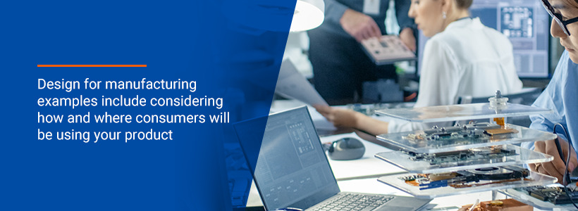
Design for manufacturing examples include considering how and where consumers will be using your product. If you develop a product for use outdoors throughout the year, the materials will need to be able to withstand the full range of ambient temperatures and weather conditions. If users will be mounting the product onto other objects, the design will need to accommodate a variety of setups.
5. Testing/Compliance
The final stage of DFM is to determine whether the design and materials for the product in question will fulfill the safety and quality standards of the various entities that have a say in the matter. A third-party ISO-certified testing facility can determine this. A neutral manufacturing analyst must oversee the testing.
Various entities could have standards that will impact your ability to go forward with a design in its current state. For example, regulatory rules at the state, federal or international levels might deem your product unsafe in its existing configuration. The product might not meet the code of its intended industry. The design of the product might even fail to meet the safety standards of your company.
Common Design Mistakes
During the design and production of PCBs, employing DFM can eliminate the following mistakes.
1. Edge Clearance
One of the most significant mistakes a manufacturer can make with a PCB design is to not allow sufficient edge clearance. This issue can be problematic for copper along the edge of a PCB, as copper can corrode if it lacks protective coating. If you design a PCB without this allowance in mind, the coating might get removed during the final cut.
Fortunately, you can easily rectify edge allowance problems if you add the necessary clearance into the design of the board. For the outer layers of a PCB, the coating should only require an additional 0.010” to the design. For the inner layers, the coating should only necessitate an additional 0.015” to the design.
2. Creating Acid Traps
Acid traps could be a recurring issue on PCB designs that fail to take this issue into account. To avoid this possibility, never design angled traces at acute angles. For example, a 45-degree angle is much more preferable than an angle of 90 degrees. The latter could render the PCB vulnerable to acid traps, whereas the former will generally not be prone to this issue. Always double-check all the trace angles after you finish the routing to ensure no joined traces have created acid traps.
3. Complicated Board Layout
If you arrive at a situation where your board becomes complex, you should rethink the design into a more solvent plan where you can organize all the necessary components on the same side. A mistake some PCB designers will sometimes make is to place a few of the elements on the flip side of the board to free up space on the primary side.
When you place components on both sides of a PCB, it increases the cost of the manufacturing process. Moreover, the addition of components on the other side of a PCB adds numerous complications for the manufacturer.
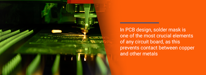
4. No Solder Mask Between Pads
In PCB design, solder mask is one of the most crucial elements of any circuit board, as this prevents contact between copper and other metals. Without the presence of solder mask between the pads, contact could form between negative metals, causing unexpected short circuits.
To ensure each circuit board has sufficient solder mask, include this in the design rules for all of your PCB productions. That way, there should never be any problems with the application of solder mask when converting the settings of a large PCB to a smaller circuit board.
5. Placing Vias in Pads
If space is tight on your PCB, you might be tempted to add vias to free up space. However, this could weaken the mounting capabilities of the PCB by drawing solder away from the board, thus rendering the soldering process ineffective. Even though the vias option can be useful in certain circumstances, only use it when necessary. The same is true for micro, blind and buried vias.
How Design for Manufacturing Translates Into PCB Layout
In PCB engineering, the principles of DFM help manufacturers keep all the design specs in a functional layout, regardless of the size of the PCB in question. When incorporating the components of one board into a smaller PCB, it can be difficult to fit the parts in place and steer clear of issues such as acid traps and problems with edge clearance. DFM helps avoid these problems before the board goes into production.
With DFM engineering, certified manufacturers inspect the design of a circuit board to ensure its measurements are sufficient for the PCB’s intended purposes. They also examine the board design to ensure it will function in its intended environments. For example, if the board will see use in machinery that generates tremendous heat, the PCB design will need to incorporate components and protective elements that can withstand these conditions.
The DFM process also ensures a PCB design will not receive approval for production if it fails to pass a series of standards tests. For example, if a PCB fails easily under a set of probable working conditions, the designer will need to re-work the board with additional components until it can handle the tasks of its corresponding devices.
In PCB production, the principles of DFM go hand in hand with design for fabrication, which covers the issues of fabrication and how it applies to a PCB.
DFM Checks From Millennium Circuits Limited
When it comes to design inspections and compliance testing, you must seek the input of an objective, qualified third party. At Millennium Circuits Limited, we run DFM analysis on PCB designs and prototypes to identify defects and other problems. Contact MCL today to learn how we can help you improve your PCBs before you put them into production.