

Printed circuit boards (PCBs) and the Internet of Things (IoT) are deeply interconnected. IoT embeds sensors and internet connectivity into physical objects, while PCBs house the electronics that enable this connectivity and data collection. We see IoT in daily life through smart thermostats, connected appliances, wearables, asset trackers, industrial sensors, and smartphone apps that serve as user interfaces or gateways.
What many don’t realize is that IoT is playing an integral role in a shift in PCB design and manufacturing. Flexible (flex) PCBs and high-density interconnect (HDI) PCBs enable smaller, more reliable, and high-performance connected devices. As IoT device demand rises, understanding its interconnections with flex and HDI PCBs becomes crucial for designers.
What Is IoT?
IoT is a network of physical objects, such as household appliances and industrial machinery, that are embedded with sensors, software, and internet connectivity. These smart devices communicate with each other and with the cloud to collect data, automate tasks, and operate without human intervention.
IoT systems we interact with every day include smartphone apps that control home appliances and utilities, wearable tech, and connected vehicles with data accessibility. IoT is also widely used in industrial environments, where it supports predictive maintenance needs.
As such, industries like manufacturing, automotive, and medical need well-designed printed circuit boards for Internet of Things devices. Specialized PCBs can help them streamline processes and enhance efficiency on a larger scale.
IoT Device Characteristics
IoT devices use sensors, processors, and communication modules to collect and exchange environmental data over networks. Components of modern IoT devices include:
- Sensors: Key to IoT devices, sensors detect and measure environmental changes like temperature, pressure, motion, humidity, and light. They convert metrics into readable digital data.
- Actuators: These receive digital commands or triggers and convert them into physical output, such as turning on a motor, opening a valve, or adjusting a thermostat.
- Connectivity: Devices must be networked to communicate data with other systems. They use different communication methods based on range and power requirements, like Bluetooth Low Energy (BLE), Wi-Fi, Zigbee, Thread/Matter, LoRaWAN, Sub-GHz ISM, Ethernet, LTE-M, NB-IoT, 4G/5G, GNSS/GPS for positioning, and NFC depending on the use case.
- Data processing: Embedded processors extract insights from collected data, analyzing telemetry to drive triggers and automate responses.
- Edge computing: Instead of transmitting all raw sensor data to a centralized cloud, edge computing processes and analyzes data directly on or near the device. This minimizes latency for real-time decision-making, reduces network bandwidth costs, and enables offline functionality even if cloud connections fail.
PCB Applications Driven by IoT
PCBs form the core of IoT devices, driving applications from smart home lighting to remote healthcare monitoring. IoT influences PCB design across industries, including:
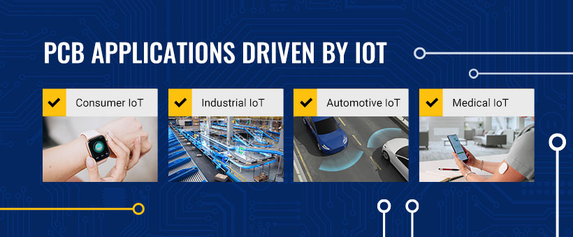
Consumer IoT
IoT drives PCBs for consumer products like smart thermostats, connected appliances, and lighting. These devices can benefit from multilayer rigid-flex PCBs, which fit hardware into tight spaces like behind light switch plates while maintaining reliable Wi-Fi, Zigbee, or Bluetooth for remote control.
Flex and HDI are among the best PCB types for wearable IoT devices like smartwatches and fitness bands. Wearables are limited by size and battery capacity. However, HDI and curved rigid-flex boards allow circuits to bend and fit comfortably against the human body.
Compact PCBs also power portable blood pressure monitors and weight scales. These boards translate sensor data into digital information for mobile app syncing.
Industrial IoT
Industry 4.0, driven by IoT, is all about the automation and interconnectedness of devices in industrial settings.
For example, PCBs process analog data from factory machinery and can resist dust, heat, and moisture in these environments. Global tracking devices and logistics tags use ultra-low-power GNSS/GPS receivers and cellular, BLE, or LPWAN-enabled PCBs to provide supply chain visibility while maintaining long battery life.
IoT can also help predict maintenance needs for industrial machines like conveyors and critical rotating assets. These systems use equipment sensors to analyze vibration patterns and temperature, triggering maintenance alerts. This helps predict failures well in advance, preventing breakdowns and downtime.
Automotive IoT
Automotive IoT, including connected vehicles and smart fleet sensors, is transforming PCB design. Software-defined vehicles need PCBs supporting higher data speeds, wireless connectivity, and increased component density. Applications include:
- Autonomous vehicles: Advanced driver-assistance systems (ADAS) use high-layer-count HDI PCBs. They process massive data from multiple cameras and sensors simultaneously in real time.
- In-car infotainment: Infotainment systems need PCBs with high-speed interconnects for AI voice assistants, high-resolution touch screens, and wireless 5G/V2X connectivity.
- Fleet management: Telematics uses connected IoT PCBs to help manage fleets. It can provide real-time vehicle diagnostics, track movement, and provide better routes for logistics or rideshare companies.
Medical IoT
In healthcare, implantable medical devices like pacemakers and neurostimulators need specialized, biocompatible, miniaturized PCBs. They must operate for years inside the human body with ultra-low power consumption.
Wearable ECG patches and continuous glucose monitors need compact PCB assemblies with qualified patient-contact materials. They typically use BLE, NFC, or gateway-based connectivity while meeting privacy, cybersecurity, and data-encryption requirements.
The IoT Opportunity for Flex and HDI PCBs
IoT is driving innovation in electronic design, moving beyond the constraints of traditional PCBs and into advanced flex and HDI PCBs. These boards provide more design freedom, allowing us to manage high-power demands within compact device spaces. When designed for harsh environments and repeated flexing, they can offer improved flexural durability, making them suitable for many IoT applications.
For instance, adherence to industry guidelines like the IPC 2223-2026 helps ensure that these flexible designs meet rigorous performance and reliability benchmarks essential for demanding IoT applications.
Advantages of Flex PCBs
Flex PCBs reduce the design limitations of traditional rigid PCBs. Their flexible structure suits various electronic shapes, reducing costs and errors due to smaller size, lighter weight, and greater durability. Advantages of flex PCBs for IoT designs include:
- Smaller size: Flex PCBs occupy less volume, making it easier to fit components like microphones and batteries into a small package without affecting performance. These PCBs can bend and conform to irregular shapes, allowing miniaturization and denser circuitry.
- Lighter weight: They can substantially reduce circuit-board and interconnect weight compared with some rigid-board, cable, and wire-harness configurations, making compact IoT products easier to package.
- Greater resistance: Flex PCBs bring better durability and resistance to impact, vibration, and environmental factors like body heat and humidity. This also makes them well-suited for industrial settings where IoT PCBs are crucial, as they can withstand harsher conditions.
- Clearer wiring routes: These PCBs simplify wiring by eliminating the need for mechanical connectors. This improves signal integrity and reduces complexity in compact IoT systems, such as connected automotive components.
You can find flex PCBs in single-sided construction for basic flexibility, double-sided for increased density, and multilayer for complex designs needing more structure. Rigid-flex PCBs are a strong combination as they integrate the rigid sections for support with flexible ones for interconnections. Millennium Circuits Limited (MCL) offers a wide range of flex PCBs, and we partner closely with engineers to ensure designs meet demanding performance requirements.
Advantages of HDI PCBs
HDI PCBs are indispensable for small-packaged personal electronics designs. Designers and manufacturers should consider their speed and reliability for IoT design. Benefits of HDI PCBs include:
- Reduced size and weight: HDI PCBs maximize electrical performance with minimal footprints. They have superior wiring density with tiny trace widths and features like stacked microvias to save board space. Smaller boards mean more uses, making them ideal for shrinking IoT devices.
- Cleaner circuit routing: HDI boards offer more versatile routing options due to blind or buried vias and microvias, smoothing out denser parts of the circuit. Designers can replace through-holes with microvias, and shorter component spacing improves signal integrity.
- Improved cost effectiveness: Greater energy and routing efficiency lead to a more cost-effective product. The HDI PCB’s smaller size can reduce board area and material use, though advanced HDI fabrication may increase process complexity.
MCL leverages advanced HDI PCB capabilities to deliver higher-performance products with state-of-the-art microvia processes and intricate stack-up designs. These PCBs can meet the demands of the most compact and complex IoT applications.
IoT Potential of Combining Flex and HDI Methods
Industry leaders combine flex and HDI strategies to create efficient and appealing designs. Some benefits of these methods include improved flexural durability, electronics better suited for harsh environments, improved signal quality, and reduced mechanical and thermal stress.
IoT requires adapting smaller devices to various uses, making the size freedom of flex and HDI PCBs essential. When configuring the best PCB for your next IoT design, brush up on the latest IoT PCB design requirements to ensure the best performance.
PCB Design Requirements for IoT Devices
Designing an ideal IoT PCB involves attention to a few key areas. Here are these areas, with tips for optimizing your PCB design for IoT:
Miniaturization and Form Factor
Small devices continue to miniaturize. HDI and rigid-flex boards now offer reliable functionality and flexibility in compact spaces. Virtual prototyping is needed to incorporate your design’s shape into its intended IoT form. Circuits must fit nontraditional materials, potentially requiring mesh or plastic in unexpected designs.
Power Management and Battery Life
IoT requires a focus on extended battery life and power integrity, since many devices periodically communicate with networks while spending much of their time in low-power sleep states. Strict energy budgeting within individual PCB circuit blocks helps the product maintain suitable power consumption.
Precisely plan power consumption, then thoroughly test your PCB’s task cycles, including transmitting and standby power states.
Wireless Connectivity and Radio Frequency (RF) Performance
The “Internet” in IoT underscores the essential need for reliable wireless access. Data transmission requires careful selection and integration of wireless modules and RF circuit components. Designers must consider power efficiency, network range, speed, and security needs when implementing connectivity solutions, alongside effective antenna design. Also consider hardware-level security, like secure boot mechanisms and elements to protect against tampering or unauthorized access.
Thermal Management and Durability
For high-performance and wearable IoT devices, conduct simulation tests and optimize PCB mechanics to account for body temperature, moisture, and movement. Pay close attention to thermal effects and ensure your design enables cooling when needed. Also, make sure PCBs are durable against impacts, vibrations, and environmental stressors.
Material Selection and Manufacturability (DFM)
Selecting the right substrate materials and copper weights is crucial, as they affect a PCB’s performance, durability, and thermal characteristics. You can improve cost-effectiveness by optimizing your production processes, minimizing material waste, and increasing yield rates. Involving a PCB partner early can refine layouts and ensure efficient production.
Collaboration Across Disciplines
It’s also important that all IoT product designers are on the same page from the beginning of the design stage. Communication and integration between PCB designers, mechanical engineers, electrical engineers, and software developers is now essential. This way, you can consider all product requirements from conceptualization to final implementation.
The Future of PCB Design for the IoT
IoT presents the PCB industry with myriad new challenges and opportunities. We are only seeing the beginning of how the two will continue to interact, blurring lines between electrical and mechanical, and creating even smaller high-performing minicomputers over time.
Future IoT PCB design will likely evolve alongside edge AI and advanced sensor integration. The global AI edge devices PCB market size is projected to grow from $15.4 billion in 2026 to $67.6 billion by 2033. Connected devices will likely require more compact layouts, efficient processing, and reliable data collection. These priorities may increase demand for PCB designs that support miniaturization, power efficiency, and multifunctional device architectures.
Alongside technological advancements, we will likely see more sustainable PCB design practices. This involves focusing on environmental considerations throughout the board’s life cycle, from material sourcing to end-of-life management, ensuring both innovation and ecological responsibility in the evolving IoT landscape.
Why Trust Us?
At Millennium Circuits Limited (MCL), we partner with innovators shaping IoT’s future. With over 20 years of industry experience, we’ve cultivated deep expertise in modern PCB design’s complex demands, especially for cutting-edge IoT applications. We understand your IoT projects require more than just standard boards — they demand the precision, flexibility, and high-density performance our Flex and HDI PCBs consistently deliver.
Our commitment is to meticulous quality and rigorous engineering, making sure every board meets the highest reliability standards your connected devices deserve. MCL offers a comprehensive service starting with a dedicated Customer Concierge who precisely fulfills your order and communicates throughout the process. Our MCL Technical Experts utilize a thorough 56-point DFM checklist to enhance design efficiency and minimize the need for redesigns during transition.
We help our customers navigate the intricate world of IoT PCB design, providing solutions that empower innovation, optimize performance, and stay within budget. Choosing MCL means gaining a trusted advisor dedicated to bringing your IoT vision to life. See how we ensure quality at all steps.
Partner With MCL for Your IoT PCB Innovation
At MCL, we print high-quality PCBs to help our customers innovate in the complex IoT landscape. From extending IoT’s reach with top-quality flex PCBs to offering the highest performance with our HDI boards, expect a high-quality solution tailored to your needs. We leverage our deep expertise in advanced flex and HDI PCBs to meet design specifications for your most demanding IoT projects.
Trust our customer service team to provide industry-leading options that exceed expectations while staying within your budget. Contact us today to get started on your next IoT-optimized project.