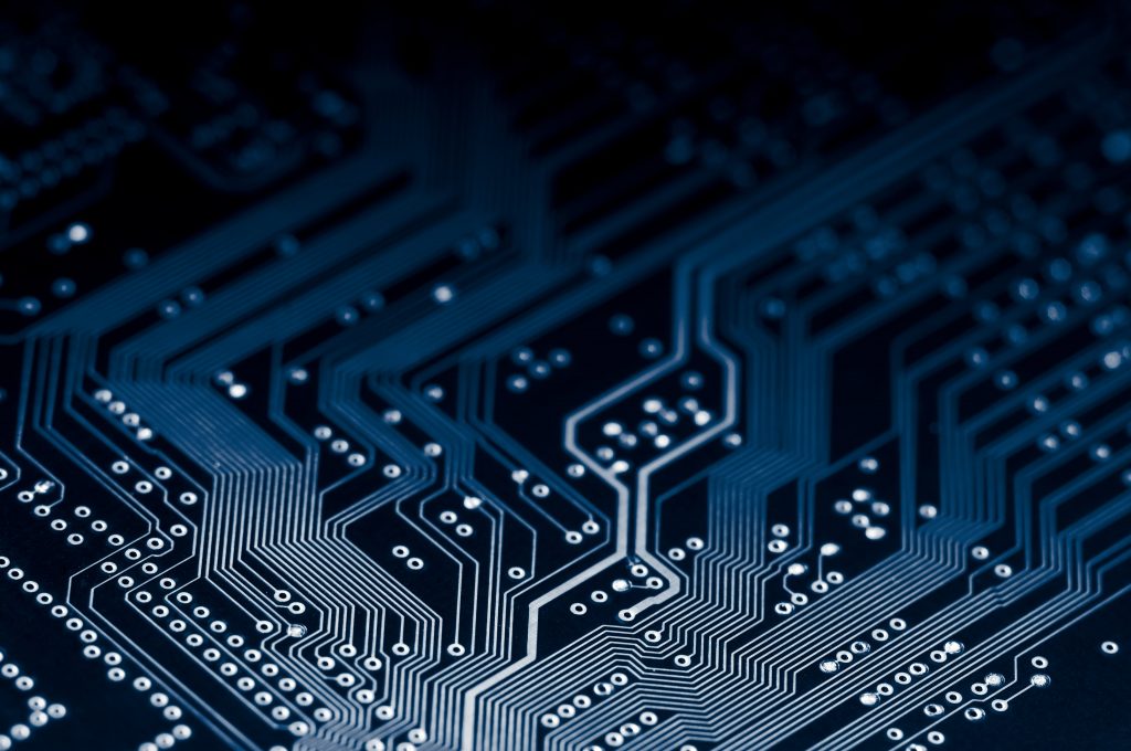
IC Packaging

IC Packaging

Jump To:

For a semiconductor to work reliably over many years of use, it is crucial for each chip to remain protected from the elements and possible stresses. That brings us to two questions – what is integrated circuit (IC) packaging, and why is it essential for your electronics applications? If you work in the electronics industry and are not clear on how IC packaging material can work for you, here is a basic breakdown of the idea behind IC packaging.


Request a Free Quote


What Is IC Packaging?

What is IC Packaging?
IC packaging refers to the material that contains a semiconductor device. The package is a case that surrounds the circuit material to protect it from corrosion or physical damage and allow mounting of the electrical contacts connecting it to the printed circuit board (PCB). There are many different types of integrated circuits, and therefore there are different types of IC packaging systems designs to consider, as different types of circuit designs will have different needs when it comes to their outer shell.

Why Is IC Packaging Important?

IC packaging is the last stage in the production of semiconductor devices. During this important stage, the semiconductor block gets covered in a package that protects the IC from potentially damaging external elements and the corrosive effects of age. The package is essentially an encasement designed to protect the block and also to promote the electrical contacts that deliver signals to the circuit board of an electronic device.

IC packaging technology has evolved since the 1970s when ball grid array (BGA) packages first came into use among electronics packaging manufacturers. At the dawn of the 21st century, newer options in package technologies eclipsed pin grid array packages, namely the plastic quad flat pack and the thin small outline package. As the noughties progressed, manufacturers like Intel ushered in the era of land grid array packages.

Meanwhile, flip-chip ball grid arrays (FCBGAs), which accommodate more pin counts than other package types, superseded BGAs. The FCBGA contains input and output signals over the whole die, as opposed to just the edges.

Common IC Package Types

There are various ways to categorize IC packaging designs based on formation. As such, there are two types of IC packages: the lead-frame type and the substrate type.

What Are the Types of IC Packages?

Beyond the basic structural definition of an IC package, further categories distinguish secondary types of interconnection. Further information about the different categories of IC packages can be found below:

  • Pin-grid array: These are for socketing.
  • Lead-frame and dual-inline packages: These packages are for assemblies in which pins go through holes.
  • Chip scale package: A chip scale package is a single-die, direct surface mountable package, with an area that’s smaller than 1.2 times the area of the die.
  • Quad flat pack: A lead-frame package of the leadless variety.
  • Quad flat no-lead: A tiny package, the size of a chip, used for surface mounting.
  • Multichip package: Multichip packages, or multichip modules, integrate multiple ICs, discrete components and semiconductor dies onto a substrate, making it so the multichip package resembles a larger IC.
  • Area array package: These packages offer maximum performance while still conserving space by allowing any portion of the chip’s surface area to be used for interconnection.

It’s important to note that many companies utilize area array packages. The foremost example in this regard is the BGA package, which comes in various formats, including the tiny chip scale packages — sometimes referred to as QFN packages — and larger packages. BGA construction involves an organic substrate, and its best application is in multichip structures. Multichip modules and packages are the leading alternatives to solutions that use a system-on-chip format. Other options include the two-stepped and double-surface interconnection packages.

Additionally, a category for wafer IC assembly, known as wafer-level packaging (WLP), has caught on in industry parlance. In wafer-level packages, the construction occurs on the wafer’s face, creating a package the size of a flip chip. Another wafer level package is fan-out wafer-level packaging (FOWLP), which is a more advanced version of conventional WLP solutions. Unlike a WLP where the wafer is diced after the outer layers of packaging are attached, FOWLP wafer dicing occurs first.

What Is the Most Common IC Package?

Lead frames are the most common IC package types. You would use these packages for wire-bond interconnected dies, with a silver or gold-plated finish. For surface-mount plastic packages, manufacturers often use copper lead-frame materials. Copper is highly conductive and extremely compliant, so it can be beneficial for this purpose.

IC Design Considerations

Choosing the right IC package for your applications starts with knowing technical information about the wide range of design considerations that go into producing IC packages. For instance, you’ll want to be aware of the right material compositions and substrates for your IC package. It’s also important to know the difference between rigid and tape package substrates. Many companies also consider using laminates as alternatives to lead frames and select substrates that work well with metal conductors.

Learn more about some of the top design considerations below.


Material Composition

The performance of an IC package relies largely on its chemical, electrical and material makeup. Despite their functional differences, lead-frame and laminate packages both rely heavily on material composition. Lead-frame packages, the prevailing format, use silver or gold wire-bond finishes, attached with a spot-plating method. That makes the process simpler and more affordable.

On ceramic packages, Alloy 42 is a widely used metal type because it works with the underlying material. On plastic packages, the copper lead frame is preferable because it safeguards the solder joint and offers conductivity. Due to policies in certain territories, the material is also one of the critical factors on surface mount plastic packages.

Because of revisions in European standards, the lead finish has been a matter of intense scrutiny on next-level packaging assembly. The aim has been to find viable replacements for tin-lead solders, which are easily applied and have been a longtime staple throughout the industry. However, manufacturers have yet to unify around a single solution, due in part to the widespread competition among suppliers. The lead issue is unlikely to resolve itself for some time to come.


Alternative to Lead Frames

Starting in the late 1970s, laminates emerged as an alternative to lead frames in chip-to-board assemblies. Today, laminates are widespread throughout the IC packaging solutions industry, due to their relative cost-effectiveness when compared to ceramic substrates. The most popular laminates are the organic, high-temperature types, which provide superior electrical characteristics and are also more affordable.


Applicable Substrates

Amid the rise in popularity of semiconductor packages, there has also been an increased demand for applicable substrates and interposers. A substrate is the part of an IC package that gives the board its mechanical strength and allows it to connect with external devices. The interposer enables connective routing in the package. In some cases, the words “substrate” and “interposer” are interchangeable.


Difference Between Rigid and Tape Package Substrates

Package substrates come in rigid and tape varieties. Rigid substrates are firm and defined in their shape, whereas tape substrates are slim and flexible. In the early days of IC manufacturing, substrates consisted of ceramic material. Today, most substrates are made of organic material.

If a substrate consists of multiple thin layers stacked to form a rigid substrate, it is known as a laminate substrate. Two of the most common laminate substrates in IC manufacturing are FR4 and bismaleimide-triazine (BT). The former consists of epoxy, while the latter is a high-grade resin material.

Due in part to its insulation qualities and low dielectric constant, BT resin has emerged in the IC industry as one of the favored laminate materials. On BGAs, BT is the most commonly used of all the substrates. BT has also become the favored resin for chip scale package (CSP) laminates. Meanwhile, competitors around the globe are manufacturing new epoxy and epoxy-blend alternatives, which threaten to give BT a run for its money, possibly reducing prices overall as the market becomes more competitive in the years ahead.

As an alternative to rigid substrates, tape substrates are mostly made of polyimide and other types of temperature-tolerant, durable materials. The advantage of tape substrates is their ability to simultaneously move and carry circuits, which makes tape substrates the preferred choice in disk drives and other devices that carry circuits amid fast, constant movement. The other main advantage of tape substrates is their low weight, which means they do not add even the slightest dimension of heaviness to an applied surface.


Substrates to Assist Metal Conductors

IC packages must also come with metal conductors that can route signals to various interconnecting features. Therefore, it is essential for substrates to help facilitate this process. Substrates route the input and output signals of a chip to other features on a system in packages. The placement of foil, typically copper, that is bonded to the laminates in the substrate achieves the metal conductivity. Immersion layers of gold and nickel often get applied as finishes over the copper to prevent interdiffusion and oxidation.


Alternate IC Package Materials and Methods for Assembly

IC Packaging Materials

Many manufacturers are trying to move away from actual lead finish lead-frame IC packages, but they have been in such frequent use for so long that it is a difficult transition for some. The most common packages include the following:

  • Dual inline packages: A dual inline package consists of two rows of electrical pins along the horizontal edges of a rectangular IC piece. A dual inline package mounts to a circuit board with either a through-hole or a socket.
  • Small outline packages: A thin small outline package (TSOP) is an IC component that consists of a rectangular shape with small pins along the horizontal edges. TSOPs are common on ICs that power RAM and flash memory.
  • Quad flat packages: A quad flat package (QFP) is a flat, square IC component with leads along each of the four edges. QFPs cannot be through-hole mounted, and sockets are rarely available for packages of this type. QFPs can have as few as 32 pins or as many as 304 pins, depending on the pitch range. Variants of the QFP include low-profile and thin. Japanese electronics manufacturers first used QFPs during the 1970s, though the package type would not gain traction in North America and Europe until the early ’90s.
  • Ball grid arrays: A BGA is a chip-carrying surface-mount package commonly seen in computer equipment. Unlike other IC packages, where only the perimeter can connect, the entire bottom surface can mount on a BGA. Due to the shorter ball connections, BGAs offer some of the highest speeds of all IC packages. BGAs are common on RAM sticks and USB cards, including RAM and speaker cards. The soldering process on a BGA necessitates precision.

Substrate packages, such as ceramic-based packages, will require an alloy that is similar in coefficient of thermal expansion (CTE) to ceramic, like Iconel or Alloy 42. In the die attachment process, we bond the die to the substrate with special die-attach materials, which we can use in face-up wire-bond assembly. It’s crucial to avoid gaps in the attached material, as these can lead to hot spots. Good die-attach material is electrically and thermally conductive, making it ideal for substrate packages.

You would use laminate instead if you need higher performance or are dealing with high I/O counts. Laminate packages are an excellent low-cost alternative to ceramic substrates and have a lower dielectric constant as well.

What Is Die-Attach Material?

This IC package type serves two primary functions. The first is to safeguard the die from damage external factors might cause. The second is to redistribute the input and output to a manageable fine pitch. Additionally, the package provides a standardized structure that directs the thermal pathway properly, away from the stacked die. Overall, the structure is better suited for electrical tests and more resistant to errors.

Die-attach materials are either liquid or film materials that manufacturers design to avoid outgassing, which could degrade the quality of the wire bond. These materials also serve as a stress buffer, so the die doesn’t fracture if the CTE does not quite match up with the substrate.

There are different methods of applying die-attach materials, some of which are more complicated than others. For the majority of uses, die-attach gets applied on assemblies where the wire bond is on the face of the surface. In all cases, die-attach materials are thermally conductive. On certain assemblies, die-attach also provides electric conductivity. To prevent spots from turning too hot along with the die, manufacturers generally seek to prevent voids in the material. Die-attach materials, both liquid and film, resist outgassing and protect dies from damage.

Wire Bond Assembly Types

Wire bond assembly types

Wire bond assemblies come in three formats:

  • Thermo-compression bonding
  • Thermosonic ball bonding
  • Room temperature ultrasonic wedge bonding

The wire bonding assembly type you choose will come with different assembly capabilities. Wire bonding typically uses gold wire, although you can use copper wire instead if you have a nitrogen-rich assembly environment. Wedge-bonding with aluminum wire can be an economical alternative.

Ultrasonic bonding starts with a wire feed through a hole in the surface of a component assembly. The process includes a die and substrate bond.

Thermosonic bonding is a process used to connect silicon ICs to computers. The process assembles the components of central processing units, which integrate the circuitry of personal computers and laptops.

Thermosonic bonds are composed of thermal, mechanical and ultrasonic energies. The machines that conduct put this process contain transducers, which transform electrical energy into piezoelectricity.

Thermocompression bonding is a method that joins two metals through a mix of force and heat. The method is alternately called wafer bonding, diffusion bonding, solid-state welding and pressure joining. Thermocompression bonding protects electrical structures and device packages in advance of surface mounting. The method includes the diffusion of the surface and grain boundary.

Encapsulants

Encapsulants are the last piece of the IC package and serve to protect the conductor and wires from environmental and physical damage. They can be made from epoxy or epoxy blends, silicone, polyimide or either solvent-based or room temperature vulcanizable. The rest of the components you choose will depend upon the specific needs of your integrated circuits and your applications.

Printed circuit boards can be vulnerable to electrostatic dust in industrial and automotive environments. To protect the mechanical properties of PCBs, manufacturers now use encapsulation resins.

As a protective barrier, potting and encapsulants are highly effective at preventing dust and other atmospheric elements from harming the mechanisms of PCBs. With sufficient resins, encapsulants can protect PCBs from the stresses of vibration, shock and external elements. For the application to work effectively, resins must get tested for their suitability in various potential working environments. The units’ functionality in these settings should also get evaluated.

As an alternative to potting and encapsulation resins, some manufacturers use conformal coatings, which snug the shape of each board and offer strength and durability, without affecting the weight or dimensions of a PCB. Coatings generally get tested in normal atmospheric settings. Each test places the effect of a given coating on the electrical and mechanical capabilities of a PCB under examination.

Encapsulant materials come in three basic varieties. The primary material is epoxy, either pure or blended. Epoxies consist of organic resins and are generally affordable, hence their popularity among manufacturers. Another widespread material used in encapsulant IC chips is silicone, which is not carbon-based and therefore not an organic resin. Silicone resins are generally solvent-based. Alternately, some resins are room-temperature-vulcanizable, and contact with moisture can cure them. Silicones are popular due to their flexibility in hot as well as cold settings.

Potting and encapsulation resins come in several different formulations, as do conformal coatings. Each formulation is balanced for a specific range of atmospheric conditions. Through testing, manufacturers can determine which formulations are best suited for particular environments. In a normal situation, most types of resins and coatings will offer sufficient protection for a PCB. In harsher settings, a board will generally require a coat with special material, such as acrylic. If the PCB is intended for use in a submerged setting, extra-strength coats are among the most suitable options.

Resins made of silicone provide optimal PCB performance in a range of environments. For PCB designs, silicone is generally preferable to polyurethane or epoxy. Between those last two, polyurethane is the more reliable material in various settings. Polyurethane resins can be effective in marine settings as protection in saltwater immersion.

Understanding IC Packaging

Understanding IC Packaging

To keep on top of the market, it is crucial to stay abreast of trends in IC packaging. This way, you can stay competitive and make the right investments in the IC packaging material market. Various market segments affect the price, popularity and availability of packaging materials. Additionally, trends on a regional scale can impact whether packaging materials rise and fall in usage in certain corners of the world.

For news, stats and information on trends in the IC market, interested parties should read the Semiconductor and IC Packaging Materials Market report, which breaks things down according to categories and applications, all within the framework of the IC industry. Experts within the industry use design data management to collect and review information on design solutions, each bringing their insights to the table as manufacturers, suppliers and retailers and providing a full picture from across the value grid.

At any given time, sudden, unexpected events can impact the market, including natural disasters, climate change, political upheavals, disruptive technology and cultural shifts. As an interested party on the IC front, staying on top of IC packaging requires you to recognize trends regarding the production, supply, export, import, pricing, integrity analysis and overall growth rate of packaging materials, and examine them regularly so you can plan, budget accordingly and protect your revenue.

IC Packaging From Millennium Circuits

As you can see, there are many elements to IC packaging for electronic systems, and as a player in the electronics industry, it’s essential to understand them and stay abreast of new developments in advanced packaging — especially regarding how they affect your components concerning performance requirements. Some aspects of IC packaging will probably remain relatively stable in the coming years, while others may change significantly, and you’ll want to stay ahead of the game. Knowing where changes are likely to come allows you to react to them better.

If you have any questions about the various types of IC packaging or anything related to circuits or printed circuit boards, contact the experts at Millennium Circuits now. We take immense pride in helping our customers have a complete understanding of the electronics we work with. We’re happy to provide you with the design and verification information you need so you can make the best decisions about electronic components for your business.


Request a Free Quote