
Table of Contents:
- What Is PCB Component-To-Edge Clearance?
- Why Does PCB Component Clearance Matter?
- Basic Panel And Multi-Board PCB Edge Clearance Guidelines
- Tips For Determining Board Edge Clearance Requirements
A successful printed circuit board design (PCB) is heavily reliant on component placement. Though there technically isn’t any right or wrong way to place components on a PCB, it’s vital that your design promotes optimal functionality.
According to the Institute for Interconnecting and Packaging Electronic Circuits (IPC), edge clearance is a vital consideration that must be addressed when placing PCB components. PCB component-to-edge clearance is often the difference between a high-functioning circuit board and a faulty one.
What Is PCB Component-to-Edge Clearance?
PCBs comprise dozens of intricate pieces, such as active and passive components, integrated circuits, power supplies and electro-mechanical components. With so many minuscule board elements, you must ensure all PCB components are properly positioned within the board to ensure reliable operation.
Edge clearance refers to the shortest distance between any components and the PCB’s edge. Parts that lie too close to the edge of the PCB can impact the board’s functionality and potentially cause damage. However, some components require closer proximity to the edge of the circuit board to operate successfully, while system interfaces like connectors and switches must be manually accessible while also touching both connecting cables. PCB component edge clearance ensures that all parts assume their proper locations for optimal function.
Why Does PCB Component Clearance Matter?
All components within your PCB must be arranged precisely within the circuitry to ensure that the board performs with optimal reliability and efficiency. Because your board will eventually need to exchange external data, it will require interface devices like connectors. These types of components are typically placed close to the edge of the PCB and their associated circuitry.
The importance of PCB edge clearance is evident in these situations. This process ensures that pieces placed near the circuit board’s edge are correctly positioned, preventing major manufacturing and performance issues from occurring. If PCB components are placed improperly without the correct edge clearance, the following problems may take place:
- Component damage: During depanelization, even the slightest circuit board bend may damage components placed too close to the edge, resulting in cracking, breaking and lifting. These issues can be easy to miss, leading to intermittent circuitry problems and tool interference.
- Airflow interference: All connectors must be correctly joined to the interface to prevent cooling and airflow obstructions within the board.
- Inaccessibility: When incorrectly placed in the PCB, larger components can inhibit human accessibility needed to occasionally debug and rework the system.
- Automation issues: Automated PCBs have various transport systems for board processing. If any components fall too close to the edge, they could interfere with numerous conveyor belts and assembly processes.
- Higher costs: Without PCB component edge clearance, you risk hiking up waste and manufacturing costs for your company.
- Poor control board orientation: Lack of PCB edge clearance can result in inadequate control board orientation, impacting depanelization methods like scoring and routing.
Basic Panel and Multi-Board PCB Edge Clearance Guidelines
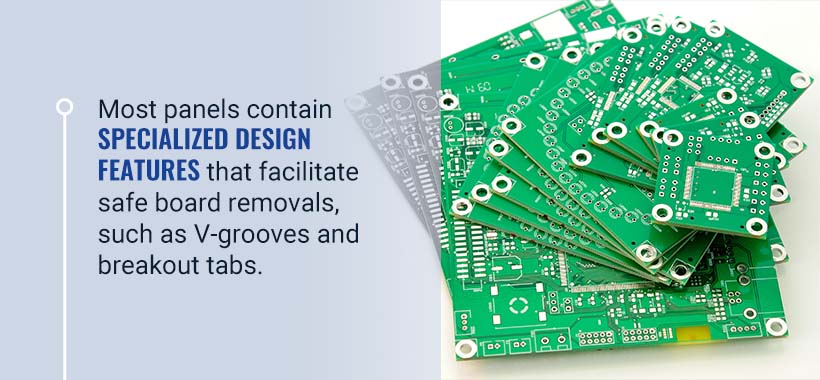
You’ll eventually have to remove your PCB panel when the assembly process is complete. When handling the circuit board, it’s important to be mindful of its various layers, including dielectric, copper, laminated core materials and all mounted components to avoid inflicting damage when depaneling the board. Luckily, most panels contain specialized design features that facilitate safe board removals, such as V-grooves and breakout tabs.
When you adhere to the following PCB edge clearance guidelines while depaneling your board, you’ll minimize the risk of damage.
V-Groove Clearances
When depaneling circuit boards with V-grooves, you’ll cut out these components using a circular cutting blade. The V-grooves will either be scored around the PCB’s top and bottom edges or routed around the board’s edge. To ensure you don’t experience issues with the pieces near the board’s edge, you can implement various clearances.
To clear the component to the board’s edge, it’s important to maintain a distance of 0.05 inches between the components and the center of the V-groove score while considering mounting variations and part size. With taller components like radical inductors, capacitors and ceramic resistors, you’ll need to allow proximity over 0.05 inches due to the position variation. You should also place elements with larger solder pads a further distance from the V-groove to prevent the solder joints from stress fracturing during depaneling.
Breakout Tab Clearances
When V-grooves cannot be used in a circuit board, perforated tabs called breakout tabs are positioned in the PCB to hold it into the panel as it’s being assembled. These tabs must be broken out of the board when depaneling, making PCB component edge clearance crucial for preventing breakage.
Breakout tabs can cause splintering and surface stress when broken out of the PCB. To prevent these effects, place the components a minimum of 0.125 inches from the perforation holes in the tabs. Taller components should remain even further at 0.25 inches from the tab.
Tips for Determining Board Edge Clearance Requirements
Determining PCB component-to-edge clearances can be tricky, as these values vary between manufacturers. However, there are some general measures you can follow, along with these helpful recommendations.
Position Drill Holes and Traces
Though drill holes aren’t considered components, it’s still necessary to clear them with the circuit board’s edge. Positioning drill holes too close to the edge of the PCB can result in cracks or breakage. You can prevent drill hole-related damage from occurring by maintaining minimal distance between the edge of the board and the edge of the hole. If you’re planning on cutting the PCB out of the panel with the V-groove method, you should create more space between the edges.
Consider Additional Physical Supports
If your printed circuit board is thicker, heavier or larger than standard devices, you might want to consider implementing different supports during manufacturing. You can add extra physical support by attaching a brace to your panel. Make sure none of the board components are positioned where the braces are needed.
Implement Copper Clearances
Copper is an active element in PCBs that isn’t considered a component but must have proper clearance between power planes and traces to the board’s edge. If this conductive metal is too close to the edge when the PCB is trimmed, the coating may be cut as well, exposing the copper layer beneath it and causing numerous functionality issues within the board. Common issues stemming from insufficient copper-to-edge clearance include shorting, corrosion and electrical shocks.
You can prevent the copper from twisting or lifting during depanelization by keeping the copper-to-edge within acceptable PCB manufacturer standards.
Ensure Proper Test Point Clearance
When conducting in-circuit tests (ICTs), the board is held in place using a vacuum drawdown to firmly join its probes to each test point. Your test points must be atleast 0.125 inches away from the edge of the PCB. This distance ensures enough space around the board’s perimeter for the test fixture’s airtight vacuum seal.
Learn More About Edge Clearance Requirements
Now that you understand the importance of PCB edge clearance, it’s time to find a high-quality bare-printed circuit board you can rely on at Millennium Circuits Limited. We’ve spent over 15 years supplying customers from numerous industries with top-of-the-line circuit boards ranging from rigid to aluminum to ceramic and more. We’re committed to delivering the best possible experiences for our customers, including rapid quote response, expert technical support and flexible lead times, all while providing cost-effective PCB products comprising the most cutting-edge technology.
Contact us with questions for our expert team today!