Updated on May 12, 2025
Table of Contents
- What Is PCB Layout?
- Essential PCB Layout Design Steps
- Understanding Design Documentation
- PCB Layout Guidelines and Considerations
- PCB Routing Best Practices
- How to Reduce Emissions and Thermal Issues in PCB Design
- Critical PCB Layout Tests
Printed circuit boards (PCBs) are the core of modern electronics, supporting and connecting all the critical components of an electronic device. Whether it is a smartphone, computer, or medical equipment, the performance of these devices depends on an effective PCB design and layout.
As electronics evolve, PCBs have become increasingly complex, compact, and performance-driven. A successful circuit board layout balances space constraints, thermal management, signal integrity, and manufacturability to achieve the highest performance. Careful planning during the PCB layout phase sets the stage for a reliable, cost-effective final product.
What Is PCB Layout?
A printed circuit board layout is the physical arrangement of traces and electrical components on a PCB. It translates the electrical schematic into a format manufacturers can use to build the board. The layout defines component placement and how copper traces, pads, and vias connect them to create functional pathways. Every decision — from trace width to component orientation — affects the final product’s performance, reliability, and cost of the final product.
A thoughtful PCB design and layout addresses signal integrity, minimizes electromagnetic interference, manages heat, complies with design standards, and facilitates efficient manufacturability and assembly. The quality of the PCB design layout often determines whether a product operates flawlessly or fails prematurely.
Essential PCB Layout Design Steps
PCB layout designing is a methodical process where decisions at each stage influence downstream performance, manufacturability, and cost. These foundational steps lay the groundwork for a reliable and efficient design:
1. Goal Definition and Conceptualization
The process begins with a clear definition of the PCB’s purpose. By defining the goal of the design and conducting extensive research, you can determine requirements for designers to work toward. These requirements include the board’s core functions, main features, the number and type of required connections with other circuits, and approximate size. Its placement in the final product and operating environment considerations, including temperature ranges, are also important considerations.
A board-level block diagram will map the high-level structure of the PCB, including the board’s final dimensions. In some cases, computer-aided design (CAD) software can be involved to create better, more compact designs, which are essential in modern PCB layout processes. These tools allow engineers to create precise schematics, design complex board layouts, manage component libraries, validate designs through simulations, and generate the manufacturing files necessary for production.
This block diagram defines how different board sections relate spatially and electrically, outlining zones for specific functions. Grouping related components in conceptualization helps minimize trace lengths and improve signal integrity.
2. Schematic Creation
After the conceptualization and establishment of requirements, the next step is translating the idea into a detailed circuit schematic. This schematic is the electrical, mechanical, and physical blueprint of the board, showing all components, their connections, and technical specifications such as voltage ratings and part numbers.
Here, engineers also create the bill of materials (BOM), listing every component necessary for production. A well-organized schematic streamlines the layout phase and simplifies future revisions and troubleshooting.
3. Component Selection and Placement
Strategic component placement is one of the most critical phases of PCB layout design. Engineers must carefully position each element based on function, accessibility, thermal management, and manufacturability. Precise placement directly impacts trace efficiency, signal integrity, thermal control, and board reliability. It is common for designers to revise placements several times to achieve the optimal arrangement.
4. PCB Routing and Draft Schematic Finalization
After placing the components, the next step is to route the electrical connections. First-pass routing involves defining trace paths that ensure minimal signal degradation and effective power delivery. Early routing decisions often reveal layout challenges that may require minor adjustments to placement or board structure.
Once the first-pass routing stage is complete, engineers conduct additional steps, including:
- Simulation
- Requirement validation
- Engineering review
These steps are repeated as needed. Then, engineers finalize the draft schematic and work on the prototype.
5. Testing and Validation
The last step is to perform a series of checks to ensure the layout meets all electrical testing requirements and works as expected. These tests include continuity, clamshell, adjacency, resistance, and capacitance testing. Any problems you find now are easier and less costly to correct than after production.
Repeat requirement validation and engineering review as needed. The design is only complete after passing all tests relevant to your needs, leading you to finalize the schematic and begin production.
Understanding Design Documentation

Throughout the PCB design process, you will create various documents that provide the technical foundation for manufacturing and assembly. Complete, clear, and organized files minimize production delays and contribute to higher-quality outcomes. Some examples of standard foundational documents include:
- Hardware dimensional drawings: Outline the size and shape of the bare board
- Schematic: Details the electrical features of the board
- BOM: Lists all the components required for the PCB, including their specifications and part numbers
- Layout file: Describes the basic physical layout of the PCB
- Component placement file: Specifies the positioning of each component on the board
- Assembly drawings and instructions: Guide the assembly process by indicating component orientation and placement details
- User guides: Optional documents offering additional information for the final user
- Gerber file set: Industry-standard files used by manufacturers to produce the board
Depending on how critical the part is, additional documentation may be required for inspections, part history, and testing performance.
PCB Layout Guidelines and Considerations
An effective PCB layout design requires careful consideration of critical factors. Some essential PCB layout best practices to keep in mind include:
Board Constraints
It’s crucial to understand the board constraints that define the physical and functional limitations of your PCB. There are dozens of possible constraints that can be linked to a PCB, but some of the most common include:
- Board size: Determine board size based on how it will fit within its final product, and plan for additional features such as mounting holes and connector clearances. If your project requires more space, you can consider multilayer or high-density interconnect designs.
- Shape: While rectangular is the most common PCB shape, irregular shapes might be necessary depending on the final product’s design.
- Number of layers: As designs become smaller and more complex, a single-layer board may no longer suffice. Complex applications with high power requirements and advanced functionality often demand multilayer boards.
Manufacturing Process
Establishing the manufacturing process to produce the board is one of the most vital PCB layout tips. Different manufacturing processes require distinct clearances, reference points, and mounting accommodations, such as design for assembly versus design for Lean Six Sigma.
Designers must consider the manufacturer’s methods and capabilities to avoid downstream production problems. When working with advanced features, such as flexible PCBs or multilayer boards, verify that the selected manufacturing partner can accommodate the design’s complexity.
Materials and Components
Establish the materials and components you plan to use on your board during the conceptualization phase. For instance, FR4 is the most common PCB base material, but for specific applications, such as high-frequency or high-temperature environments, materials like ceramic may be more suitable.
Proper thermal management is also a vital consideration when choosing materials and components. High-power components generate significant heat, so position them with adequate space for heat dissipation or near heat sinks. Lastly, make sure your chosen components are easily available and within budget. Availability influences the overall cost and lead time for your project.
Component Placement Order
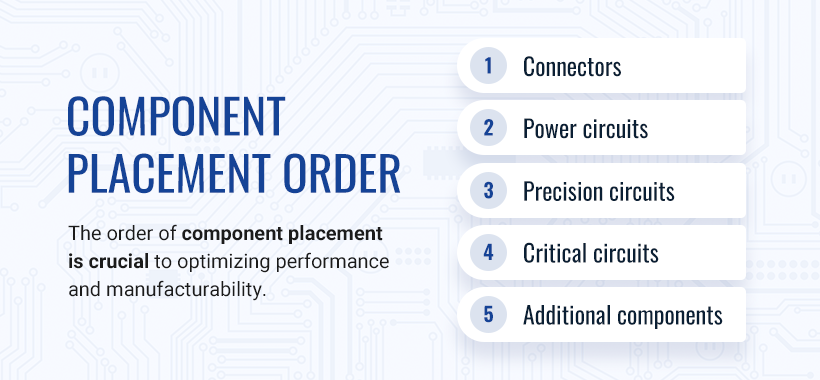
The order of component placement is crucial to optimizing performance and manufacturability. When possible, incorporating high-level, critical parts last is ideal. Through testing and validation processes, you can replace faulty or incorrect components as needed, without incurring significant rework costs.
Generally, you can follow this sequence when placing components:
- Connectors
- Power circuits
- Precision circuits
- Critical circuits
- Additional components
Component Orientation
Consistency in component orientation dramatically reduces assembly errors and is a central step in design for assembly. Align polarized components, such as diodes and capacitors, in the same direction where possible. Keeping similar components facing the same way simplifies visual inspection, aids automated optical inspection systems, and speeds up hand or machine assembly.
Layout Organization
Part of design for manufacturing (DFM), logical layout organization directly impacts cost and production yield. For instance, placing surface mount devices on one side of the board when feasible simplifies soldering and reduces manufacturing time. It is also good practice to reserve clearances around mounting holes and along board edges, and avoid placing critical traces or pads too close to these areas to prevent mechanical damage during assembly.
4 PCB Routing Best Practices
Routing and signal management are critical in PCB layout design. Applying thoughtful PCB routing techniques helps maintain strong signal quality and prevents unnecessary issues during manufacturing or field use.
1. Minimize Signal Interference and Crosstalk
To maintain signal integrity, minimizing interference between traces and ensuring a clean path for signals is critical. Here are some tips you can adopt:
- Space traces generously: Adequate spacing between signal traces prevents electromagnetic coupling and minimizes crosstalk, improving overall signal clarity.
- Avoid parallel traces: Avoid routing signal traces parallel to each other to reduce mutual inductance and the potential for signal interference. When necessary, cross traces at right angles to minimize coupling.
2. Consider Your Power, Ground, and Signal Traces
The thoughtful planning of power and ground planes, as well as signal trace design, enhances mechanical stability and electrical performance. Here are some effective PCB routing guidelines you can implement:
- Use solid power and ground planes: Centered and symmetrical power and ground planes reduce board warping and minimize electromagnetic emissions. Internal plane layers provide a low-impedance return path for signals. Large ground planes can also shield the circuitry and prevent interference.
- Ensure proper trace widths: Sizing traces based on the required current load helps prevent overheating, excessive resistance, and signal degradation across the PCB. Make sure traces are analyzed so they do not accidentally form antennas that operate on a similar frequency as the circuit.
- Use multiple vias for high-current paths: Distribute high current loads across multiple vias when transitioning between layers. This technique lowers resistance and improves thermal conductivity.
3. Control High-Speed Signal Routing and Impedance
High-speed signals are sensitive and require precise routing and impedance management to maintain signal quality.
- Route high-speed signals over solid ground planes: Always route high-speed traces directly above continuous ground planes to maintain consistent impedance and signal fidelity.
- Use 135-degree trace bends: Avoid using 90-degree trace bends, as these can cause signal reflections and degradation, especially at higher frequencies. 135-degree bends provide smoother signal flow.
4. Place Components and Traces Strategically
Positioning critical components and routing traces logically enhances signal flow and board performance, though you may have to deviate from this approach.
- Strategic component placement: Place critical components like high-speed integrated circuits (ICs) or power components in positions that minimize trace lengths and avoid thermal interference.
- Route signals based on flow: Ensure signals flow in the same direction from input to output, keeping trace lengths short and direct for optimal performance.

How to Reduce Emissions and Thermal Issues in PCB Design
Controlling emissions and managing heat generation are essential for maintaining board stability, extending product life, and achieving compliance with electromagnetic compatibility requirements.
Minimizing Electromagnetic Interference (EMI)
In addition to surrounding components with ground traces and planes, the following layout and grounding strategies substantially reduce emissions and improve circuit performance:
- Separate digital and analog grounds: Physically separate analog and digital ground planes to minimize interference between high-speed switching signals and sensitive analog circuitry.
- Use guard fences: Surround sensitive components and signal traces with grounded guard fences to shield them from external EMI.
- Leverage a stack-up design: Implement an adjacent pair stack-up design, where signal layers are immediately adjacent to ground planes. This practice reduces loop area size and minimizes emissions.
- Add series termination resistors: Adding series resistors at signal sources dampens reflections and prevents ringing that could otherwise distort signals.
- Segregate input/output (I/O): Allocate a distinct area of the PCB for I/O connectors and circuits. Segregation minimizes cross-coupling between internal signals and external disturbances.
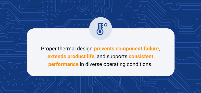
Thermal Management Considerations
Proper thermal design prevents component failure, extends product life, and supports consistent performance in diverse operating conditions. Along with looking at considerations like airflow and substrate material, here are some thermal management best practices:
- Use thermal reliefs and vias: Thermal vias and relief patterns around power components help dissipate heat and avoid thermal issues.
- Distribute heat through copper pours and heat sinks: Incorporate copper pours and heat sinks, especially around high-power components, to evenly distribute heat and assist in efficient thermal management.
Critical PCB Layout Tests
Testing is a vital part of the PCB layout process, helping identify potential issues before the design moves into manufacturing. Running comprehensive layout checks early protects against costly production delays, ensures better yield rates, validates compliance with manufacturing and industry requirements, and supports a smoother path to market.
Two essential tests every design should pass include:
Electrical Rules Check (ERC)
An ERC verifies the electrical connections between components on your PCB design, ensuring no conflicts such as shorts, missing connections, or incorrect pin configurations. This test helps confirm the electrical integrity of your design and highlights potential issues that could cause the board to fail in real-world applications.
Design Rules Check (DRC)
A DRC compares the physical layout against predefined manufacturing constraints such as minimum trace widths, feature spacing, hole diameters, and component clearance.
Once a board passes both ERC and DRC without violations, it is important to conduct a manual inspection to verify that the layout aligns with the schematic.
Why Trust Millennium Circuits Limited (MCL)
Since 2005, MCL has been a trusted global supplier of bare printed circuit boards, serving industries ranging from automotive to medical electronics. We support customers by providing technical expertise, rapid quote responses, flexible lead times, and top-tier customer service.
Whether you need prototypes, production quantities, or advanced designs like flex, rigid-flex, or ceramic core PCBs, MCL delivers diverse solutions aligned with your product’s performance goals. We are ISO 9001:2015 certified and offer competitive domestic and offshore supply options. Our products comply with various standards depending on your needs, including IPC-A-600, RoHS, REACH, and AS9102, and we follow extensive quality control and assurance protocols to verify the quality of every board.
We support every stage of your project with comprehensive engineering services, including DFM reviews, cost consulting, and life cycle management.
Learn More About PCB Layout Design With MCL
PCB layout design is an intricate, critical process that requires a deep understanding and consideration of various factors, including signal integrity, thermal management, power distribution, and emission reduction. By following PCB design best practices and using the right tools, you can create efficient and reliable PCBs that meet your application’s demands.
Reach out to MCL today to learn how we can help bring your PCB concepts to life with technical excellence and responsive service.
Summary
Key Takeaways
- PCB layout translates the schematic into a physical design, defining component placement and copper routing that determines performance and manufacturability.
- Component placement is one of the most critical steps, as positioning directly impacts signal integrity, thermal performance, and routing efficiency.
- Effective layouts balance multiple constraints, including space limitations, signal integrity, EMI reduction, and heat management.
- Routing strategy plays a key role in performance, with careful trace design helping minimize interference, crosstalk, and signal degradation.
- Ground planes, power distribution, and stack-up design are essential tools for reducing emissions and improving overall stability.
- Early design decisions have downstream impact, influencing manufacturability, yield, and long-term reliability.