
Table of Contents:
- Don’t Rely On Your Autorouter
- Route High-Speed Signals Over A Solid Ground Plane
- Place Vias In A Grid To Avoid Hot Spots
- Use A 135-Degree Trace Bend
- Increase The Spacing Between Traces To Avoid Crosstalk
- Implement Daisy Chain Routing To Avoid Hot Spots
- Do Not Route Signal Over A Split Plane
- Reduce Noise By Separating Analog And Digital Ground Planes
- Split The Layouts Virtually Between Analog And Digital Grounds
- Avoid Broken Connections With The Proper Trace Width
One of the most critical aspects of the printed circuit board (PCB) design and layout process is knowing how to route your board correctly. Implementing proper PCB routing best practices can save you time and help reduce the number of issues later in the manufacturing process.
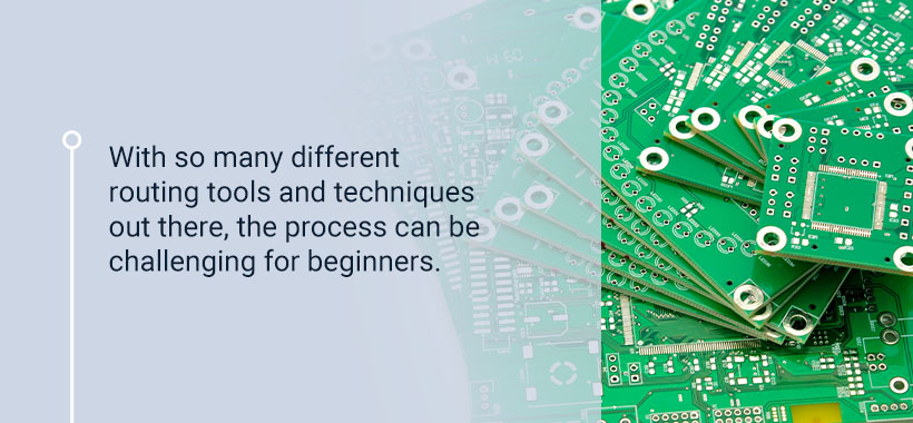
With so many different routing tools and techniques out there, the process can be challenging for beginners. Here are a few tips to keep in mind when starting to route your PCB.
1. Don’t Rely on Your Autorouter
If you’ve ever used PCB design software, you’ve probably come across an autorouter tool. At first glance, this tool may seem like a time-saver and an effective solution for routing your PCB. However, you should never rely on this tool alone. Although beginners may use this tool when learning how to route a PCB, you will see the best results by routing the board yourself.
Moreover, autorouting does not always present an accurate result. Use of the tool often results in common symmetrical mistakes, which can lead to quality issues and more routing problems on your end. It’s best to use this tool alongside manual routing and not as a standalone solution.
2. Route High-Speed Signals Over a Solid Ground Plane
When dealing with high-speed signals, it’s essential to route over a solid ground plane. Doing so ensures that the trace connection remains solid and other problems don’t occur later once the PCB is finished.
Routing PCBs over a solid plane can also help reduce the chance of impedance that likely occurs with two different ground planes. Essentially, following this best practice simplifies the process of connecting trace components to the right spots on the board.
3. Place Vias in a Grid to Avoid Hot Spots
The placement of vias is a vital aspect of PCB routing. An incorrectly placed vias can cause hot spots — regions where current density increases substantially. The increase in heat across a specific region of the board can result in severe problems.
The best way to avoid these hot spots is to place the vias within a grid to space them out across the area on the board. For the best results, you should leave at least 15 mils of space between the vias.
4. Use a 135-Degree Trace Bend
Whenever possible, avoid using a 90-degree trace bend when routing your printed circuit boards. This angle results in a trace width that is narrower than the recommended standard. While this may not seem like a significant issue, it can lead to several problems with the final layout of the PCB. The narrow outside edge of a 90-degree trace bend is also a heat trap that has the potential to cause shorts.
It’s best to route trace bends at 135 degrees. This wider angle will ensure that your board has a proper layout and avoids short issues.
5. Increase the Spacing Between Traces to Avoid Crosstalk
The spacing between traces is another crucial factor to consider. Proper spacing ensures that there isn’t a signal buildup between two traces in a single area of the board.
The increase in activity caused by improper trace spacing is known as crosstalk. When crosstalk occurs, one trace signal essentially overpowers the other. As a result, there is a chance for circuit shorts once the PCB routing is finished.
While routing your PCB, it’s best to incorporate the right about of spacing between traces to avoid this type of issue.
6. Implement Daisy Chain Routing to Avoid Hot Spots
Another way to avoid hot spots when routing a PCB is to implement daisy chaining. Daisy chaining is a routing technique that creates a connection between different points on the circuit board. This type of PCB routing helps avoid long stub traces that often cause problems with the signal being transferred.
Daisy chaining also ensures proper spacing for the signal to pass through, making it a good routing style to use when trying to avoid hot spot issues.
7. Do Not Route Signal Over a Split Plane
When routing over two different reference planes, it’s important to consider the path of the return signal between traces. Make sure the signal can correctly transmit along the return path. Routing over a split plane can also increase the likelihood of crosstalk, leading to more trace signal issues.
8. Reduce Noise by Separating Analog and Digital Ground Planes
Separating the analog and digital ground planes makes it easier to see which components must connect to the appropriate plane. In other words, separating these two sections ensures the proper connection between the respective digital and analog components. Essentially, the purpose of separating these two components is to isolate the two signals, avoid interference and reduce noise.
9. Split the Layouts Virtually Between Analog and Digital Grounds
Virtually splitting the analog and digital components of a PCB is also an effective best practice to follow when routing. Rather than physically separating the two parts, the planes are split by a virtual line. This provides an easy way to see the connections between each of the respective planes visually.
While routing the PCB, it’s essential to consider this virtual line to separate the digital and analog traces. Virtually splitting the two grounds can help keep the different signals of the PCB on the right side of the board.
10. Avoid Broken Connections With the Proper Trace Width
Understanding the proper trace width when routing your PCB can save you a lot of time and energy trying to correct problems. Without the appropriate width, the amount of electricity running through the traces can cause excessive heat to build up across the board. This increase in heat can cause the connection running between the traces to fail.
Making sure to correctly identify your trace width before routing your PCB can help reduce the risk of overheating and the chance of broken connections.

Learn More About Routing PCBs
When you understand the best practices of routing PCBs, the design and layout process becomes much simpler. Following these common tips for routing PCBs can also help save you from having to deal with issues later on in the design process.
Need help with routing for your printed circuit boards? Millennium Circuits Limited can help. We have a range of PCB capabilities to meet the needs of your project, and we pride ourselves on providing outstanding customer service. To learn more about MCL and our many capabilities, contact us today to request a quote.