
The Fundamentals of Printed Circuit Board Fabrication
With any manufacturing operation, the longevity and functionality of a product are largely determined by the quality of construction. Printed circuit boards, or PCBs, are no different.
The PCB fabrication process produces the bare printed circuit board, one of the most important features of any product. As such, the manufacturing process is a key component of the electronics production lifecycle and plays a significant part in the overall success of a project. To make the most of this process, however, customers need to understand the answers to three core questions:
- What is PCB fabrication?
- Why is it important?
- How does fabrication play into the PCB assembly process?
About PCBs
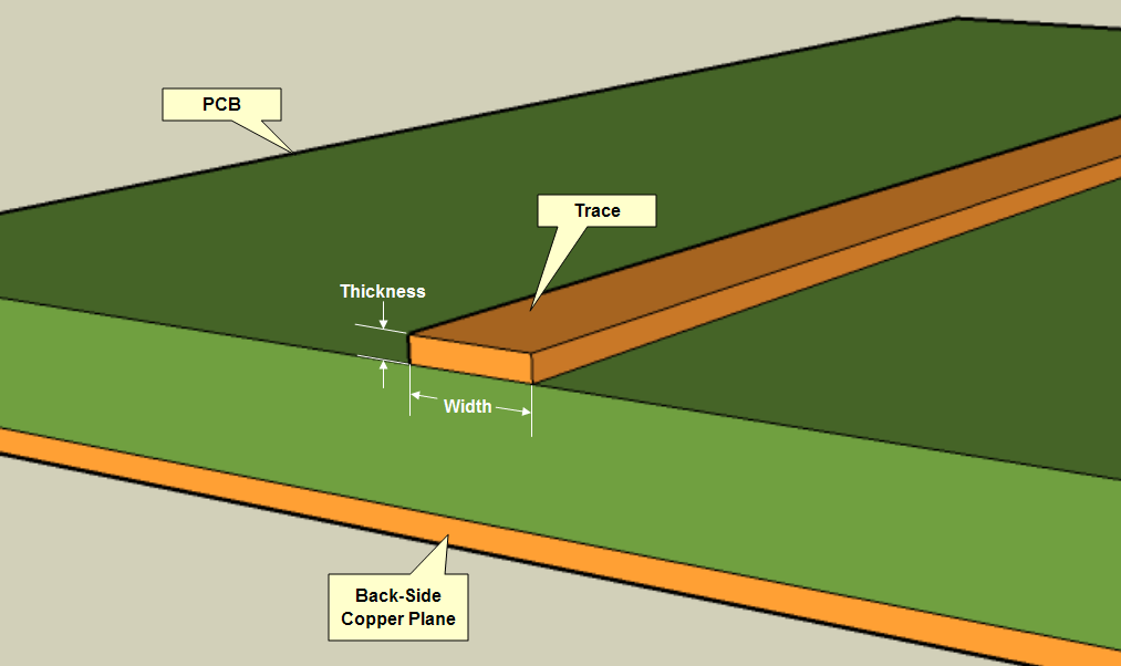
A printed circuit board carries electrical circuits and allows signals and power to be routed between devices. PCBs consist of several layers of material:
- Substrate: At the core of the board is a substrate or base material. Traditional boards use a fiberglass material called FR4, though other boards may use aluminum, ceramic or polymer substrates.
- Copper: The substrate of the PCB is covered with a thin copper foil and laminated with heat and adhesive. The number of “layers” in a board is determined by the number of copper layers — for example, double-sided PCBs will have copper applied to both sides of a substrate, and a four-layer board will have four layers of copper total. Most PCBs contain one ounce of copper per square foot, though high-power PCBs may use two or three ounces.
Get Pricing and Lead Times
These materials are combined in the fabrication process to create the bare PCB. This bare PCB is then sent through the assembly process, or PCBA, to apply solder and the electronic components, ending in a fully functional PCB.

What Is PCB Fabrication?
PCB fabrication is the process by which the aforementioned materials of a board are combined into functional layers to form the bare printed circuit board. The fabrication of bare printed circuit boards works as follows:
- Design review: The fabrication process does not start until the engineering team reviews the design. This is called a Design for Manufacturability check, which ensures the design is valid and fulfills the tolerances and specifications can be met during manufacturing.
- Film application: The PCB design is printed onto films using laser direct imaging, which provide photo negatives of the board layout. These films are applied to the material layers and used as a guide for each manufacturing process.
- Copper etching: Using various methods, the unwanted or excess copper is etched or removed to create traces and pads. This process usually involves multiple rounds of cleaning to remove excess material and unwanted chemicals.
- Layer stack-up and lamination: If the board is a multi-layer board, the inner and outer layers are aligned with one another after the copper etching process. This is usually accomplished using alignment holes in the board itself. After inspecting the layers, an epoxy-based prepreg is placed between each layer, and the board is laminated together by applying heat — the heat melts the epoxy and adheres the layers together.
- Drilling: After the board layers have been laminated together, a drill is used to create holes through the board. These holes are used for mounting holes, through-holes and vias.
- Plating: Once drilling is complete, the board is plated with a micron-thick layer of copper, which coats the inside of the drilled holes, creating plated through-holes. This is usually followed up with more etching and copper removal on the outer layer of the board.
- Solder mask application: After the copper layers are complete, the panels are cleaned and covered with solder mask. Solder mask give the PCB its characteristic green color. The solder mask insulates copper traces from accidental contact with other conductive materials that could create functional issues and helps during assembly so that solder is only applied to the correct locations. Once applied, unwanted areas of the solder mask are removed, and the PCB is placed in an oven to cure the solder mask layer.
- Silkscreen: Whether or not this is needed, the next step is the application of the silkscreen, after which point the board undergoes the final curing stage.On top of the solder mask layer, is where the silkscreen layer is applied. Silkscreen is usually white in color and adds letters, numbers and symbols to the PCB. This silkscreen layer helps assist with component type and location during the assembly of the PCB.
- Surface finishing: After the solder mask and silkscreen are cured, the PCB may be plated with gold or silver or other surface finish to ensure protection and functionality.
After the boards complete these steps, they typically undergo electrical reliability testing to ensure they are functional. After that, if the boards were produced in a panel, they are cut apart, inspected and repaired as needed.
How Fabrication Falls Into the Overall Manufacturing Process
Fabrication is only one step in the PCB manufacturing process. To fully understand the importance of printed circuit board fabrication, it’s important to know where it lies in the cycle.
The PCB manufacturing process falls within three general stages, described in more detail below:
- PCB development: PCB development is the initial stage of the manufacturing process. Essentially, this is where the PCB design is conceptualized, modified and finalized. PCB development usually includes multiple rounds of design, prototyping and testing, especially for more complex designs.
- PCB manufacturing: After the PCB design is finalized in the development stage, the PCB moves on to the manufacturing process. Manufacturing involves two steps — fabrication and assembly. Fabrication produces the design of the board, while assembly applies components to the board’s surface. At the end of this process, the boards are complete.
- PCB evaluation: The final stage of the manufacturing process is an evaluation. This includes a final round of testing after the manufacturing process is complete. This testing stage evaluates the assembled board’s ability to perform as intended and eliminates boards that fail the tests. In some cases, testing may reveal that the board requires a design adjustment, and the cycle starts over. If boards pass the tests, they undergo a final inspection for any defects before being sent out.
Why PCB Fabrication Is Important
PCB fabrication is an outsourced activity performed by a third-party manufacturer using the designs provided by their customers. Fabrication is important to understand because manufacturers only see the design, not the performance intended for your design. If designers do not keep the fabrication process and limitations in mind during the design process, fabricated boards may be impacted in the following areas:
- Manufacturability: Design choices impact the manufacturability of PCBs. Board designs need to take into account the material properties of the board and allow adequate clearance between surface elements. If the board needs to be produced in panels, this should also impact the final design. Designs that neglect these factors may be impossible to fabricate without redesigns.
- Yield rate: In some circumstances, boards can be successfully fabricated using the existing design. However, certain design choices may result in fabrication issues that render multiple boards unusable — for example, stretching the tolerance boundaries of your manufacturing equipment.
- Reliability: Most boards are regulated under industry specifications, which dictate a required level of performance reliability. Failing to follow industry requirements in design may result in unreliable or nonfunctional boards.
The best way to avoid these issues is to consider the PCB fabrication process during the design cycle. You can do this by utilizing design for manufacturability (DFM) rules and checking the capabilities of your PCB manufacturer during the design cycle. When you partner with a high-quality PCB manufacturer, you can work closely with them to help optimize your design for the PCB fabrication process.

Choose Millennium Circuits Limited
If you’re interested in working with a valued-added distributor that offers innovation as well as quality, Millennium Circuits Limited (MCL) can help.
We supply state-of-the-art printed circuit boards for many different products and across several industries. Prompt service is our standard. MCL provides same-day quotes to help increase our customer’s operational efficiency. Our relationship-driven customer service allows us to stay on top of customer’s upcoming projects, eliminating bottlenecks, and saving time.
Strategic manufacturing locations enable MCL to provide our customers with a wide spectrum of circuit board solutions with flexible lead times at competitive prices.
Contact Millennium Circuits today to learn more about the PCB fabrication process and how we can assist with your PCB needs.