In electronics and computing devices, the circuitry is conducted by a tiny green board that transfers various signals from the control prompts and to the screen. In every smartphone, for example, a printed circuit board (PCB) can be found inside with various chips and components that conduct the signals for thousands of different features and commands. Each time you push one of the prompts on the touchscreen, you are activating one of the signals on the internal board. Most of these signals are conducted through PCB vias.
Jump To: What Is a Via? | Main Types of Vias | How to Determine the Right Via Requirements for Your PCB
What Is a Via?
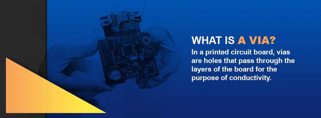
In a printed circuit board, vias are holes that pass through the layers of the board for the purpose of conductivity. Each hole functions as a conductive path through which electrical signals are passed between circuit layers. Vias travel through varying levels on a printed circuit board. Depending on the design of the PCB, the board might require a hole that goes through all of the layers from top to bottom. Alternately, some vias penetrate only the top or bottom layer, and some are placed though an inner layer. There are various options when it comes to vias on a printed circuit board.
Vias are among the most crucial features on a printed circuit board. Consequently, they account for a sizable share of the cost involved with board manufacturing.
Despite the fact that these different types of vias serve the same basic purpose, one particular type of via will be more suitable than others on certain PCB designs. This article covers the different types of vias in PCB design and how each can facilitate an electrical connection on a printed circuit board.
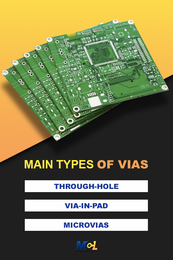
Main Types of Vias
 There are two primary categories of vias, depending on where they are in the PCB layers — the blind hole and the buried hole.
In a blind hole, the hole penetrates the top or bottom layer of the board but stops before any of the internal layers. Blind holes are named as such because you cannot see through them when you hold a board up to the light. The process involved with blind-hole creation can be difficult because you must know when to stop drilling into the board. As such, many PCB manufacturers avoid hole plating of this type.
Another type of via is the buried hole, which might appear through one or more internal layers. Since the buried hole is sandwiched between layers, it cannot be seen by the naked eye. For a multi-layer board to have a blind layer, the hole plating on the internal layer must be completed early on during PCB assembly, before the top and bottom layers are applied to the board.
Wherever the via is placed, it is likely to be one of three main types:
- Through-hole
- Via-in-pad
- Microvia.
1. Through-Hole
The most obvious type of via is the plating through-hole, which penetrates all the layers in a multi-layer board. Through-holes are typically larger than blind holes and buried holes and are also a lot easier to identify with the naked eye. When you hold a board up before the light, the light will pierce right through a plating through-hole. Through-holes are also easier to make because you can simply drill right through all the layers, unlike with blind holes, where you have to be careful how deep you make the hole.
Through-hole technology has been around since the mid-20th century when it replaced point-to-point construction. Through-holes were most common between the 1950s and 1980s when nearly all the features found on a printed circuit board were attached to a through-hole.
In the early days of through-hole technology, PCBs had their tracks printed only on the top side. As technology advanced, the printing appeared on both sides. Eventually, multi-layers boards came into use. At this point, through-holes were updated to plated through-holes to enable contacts between conductive layers. Today, plated through-holes are used to connect the different layers in a PCB. Through-holes are usually used to facilitate components with wire leads. Axial-leaded components are placed through these holes and used to connect across short spaces.
Through-holes can often be seen on the large motherboards that were used in computer towers during the 1990s and 2000s. PCBs with through-hole components could also be seen in the old peripheral component interconnect (PCI) cards that were plugged into these older motherboards. For example, the sound cards that connected to PCI slots inside the tower would typically feature components that were attached to the board in through-holes. Similar features could be found on graphics cards in the older computers that predate today’s all-in-one flat-screen devices.
With the growing popularity of small, compact, mobile computing devices and electronic gadgets, PCBs are being designed with few, if any, through-hole components. As such, there are few remaining reasons for PCB designers to continue using boards that contain large through-holes, as these consume lots of space on a board that could be put to more efficient use with microvias. In fact, for designers to keep their boards small, microvias and surface mounts should be used as much as possible. As the trend continues, through-holes will likely be phased out entirely in the years ahead.
2. Via-in-Pad
One of today’s more popular designs for printed circuit boards involves the application of vias on ball grid array (BGA) pads, alternately known as via-in-pad. In the via-in-pad design, the vias are placed on the BGA pads of the PCB. The design has become popular because it makes it possible for manufacturers to minimize the amount of space required for vias. As such, via-in-pad allows manufacturers to make smaller printed circuit boards that require less space to route signals. Via-in-pad is an optimal technology for today’s compact electronic and computing devices, which manufacturers have designed to fit into pockets and sometimes around wrists.
The via-in-pad design is especially convenient for routing because the holes connect straight to the layer that underlies the component, making it possible to route signals without the risk of going outside the perimeter of the device’s footprint.
Granted, not all manufacturers have embraced the practice of placing vias on BGA pads. One of the main drawbacks for some PCB makers is that you have to fill the pad with pure copper or some non-conductive material covered with copper. Otherwise, the solder will bleed off the pad and cause the PCB to lose its connectivity.
Another prohibitive factor for some manufacturers is the fact that vias require an additional step that can often be costly and time-consuming. Some designers simply do not wish to add to the cost of PCB creation. Moreover, when you place vias in a pad, it alters the required drill diameter.
Despite these issues, there are various advantages of placing vias on BGA pads. Costs aside, you can make smaller boards with via-in-pad and ultimately make smaller devices. For certain modern gadgets and mobile devices, the via-in-pad design might be your only option.
In a standard via layout, solder mask can be applied to stop the flow of solder into the via. With the via-in-pad design, you cannot leave the barrel free of filling because air could get trapped, causing out-gassing while the PCB is in production. Therefore, the vias need to be filled when placed on BGA pads. For the design to work, you must also have a flat planar surface, as this will make it possible to connect fine-pitch BGAs with little, if any, complications.
In-pad vias can be filled with epoxy. This should be done after the drilling and plating steps. Another option is to fill the vias with copper. This would work if the vias are laser-ablated. Whichever method you choose, you would need to make sure that the pad is large enough for the diameter of the hole and also have sufficient tolerances. Furthermore, the design would need to fulfill the IPC Class 2 and 3 standards.
If you are still in doubt as to whether via-in-pad would be the better option than a standard via layout, you should speak with a PCB manufacturer to see how the newer technology has transformed their boards.
3. Microvias
In PCB design, vias that are under 150 microns are known as microvias, which are used on many high density interconnect (HDI) boards. Designers prefer microvias because of the small size of the hole, which consumes far less space on the board than the holes that require more drilling. In a microvia, the layers are connected to one another with copper plating.
Microvias are created in the shape of cones, which makes it easy for the via sides to be copper plated. A microvia can go through two adjacent layers but not any further. If a board design requires a via through multiple layers, multiple microvias would need to be stacked accordingly.
From a manufacturing standpoint, creating stacked microvias can be a costly and time-consuming process. On boards that require one microvia over another, the most common design will feature two microvias. As far as stacking is concerned, the ultimate limit is four microvias. However, four microvias are rarely applied in PCB manufacturing because of the high costs.
An alternative option to the stacked microvia is the staggered microvia, which is set up like a staircase where a second or third microvia is placed a step forward below the one above. As with stacked microvias, staggered microvias can be difficult and costly to produce on a multi-layer PCB.
If a microvia enters through the outer layer of the board and cuts to an inner layer before stopping, that would qualify as a blind microvia. With a blind microvia, you can increase the density of the wiring on a printed circuit board. Blind microvias are especially advantageous if a signal on the outer layer must be routed to an underlying layer, as the blind microvia will offer the shortest distance. On an HDI board, blind microvias make it possible to optimize space in a multi-layer board, such as in a PCB with four layers where the microvia could be placed on either the top-two or bottom-two layers.
In some cases, a microvia will penetrate two whole layers. The blind vias that fit this description are known as skip vias. However, skip vias are not recommended by manufacturers because the nature of the hole can result in complications with plating.
A microvia that connects two inner layers in a PCB is known as a buried microvia. For a buried microvia to be included in a PCB design, the layers that contain the holes must first be drilled before the outer layers are applied. With a buried microvia, you can connect two inner layers on a printed circuit board. The drilling can be accomplished with a mechanical tool or, alternately, with a laser.
When you place a microvia on a PCB, it is crucial to pay attention to the aspect ratio of the hole size, otherwise, it might be impossible to plate the board properly.
How to Determine the Right Via Requirements for Your PCB
The type of vias that you choose for a PCB design should be based on the size and purpose of the board. If the board is made for use in an older, larger computing device, you will probably need to have a PCB design that conforms to older standards, as anything newer would likely be incompatible with the device in question. For some of these older devices, your only option would likely be a larger PCB with through-hole components.
If you are designing a PCB for a smaller device, there is really no reason to use through-hole components since you will need to maximize the small amount of space on the tiny board that would fit the device. For example, if your PCB design is merely a square inch in size, you will not have the necessary space for a large through-hole since there will be too many signals to conduct in the small amount of space allowed. A board of that size would be much better served with blind microvias, which could pass powerful signals between short distances on a thumb-sized board.
Granted, the process of making a smaller PCB with microvias will likely require more of an investment due to the labor that such boards entail. However, the advantages of these smaller boards can easily pay back the investment, especially if you are marketing a new and groundbreaking device that could ultimately become a big seller.
PCB Products and Services From Millennium Circuits

When it comes to the design of printed circuit boards, there is an array of vias to choose from, such as blind and buried microvias. On today’s smaller PCBs, microvias make it possible to equip a device with numerous features and also offer speeds and processing power that exceed the performance capabilities of the bulkier through-hole components that were commonplace 20 years ago. To produce the most compact and optimal PCB designs, it is crucial to have a team that can put these pieces together. Contact Millennium Circuits for a quote on PCB products and services.