

As AI and optical networking push bandwidth higher, PCB manufacturers are being asked to do more with less.
The rapid growth of AI infrastructure, hyperscale data centers, high-speed networking, and silicon photonics is changing the requirements for the PCBs inside today’s most advanced electronic systems.
Optical modules are moving toward higher bandwidth and greater density. AI infrastructure is demanding faster interconnects and lower latency. At the same time, engineers are being asked to fit more routing and functionality into increasingly compact designs.
That creates a fundamental question:
Can your PCB manufacturing process keep up with the design you’re trying to build?
For some applications, conventional PCB fabrication—or even increasingly advanced imaging and fabrication processes—may eventually become a limiting factor.
MCL helps engineering teams evaluate those challenges early and identify the manufacturing technology best suited to the application. For designs requiring exceptionally fine geometries, high routing density, and advanced signal performance, that may include Modified Semi-Additive Process (MSAP).
The PCB Challenge Behind the Optical Networking Revolution
The transition to 800G and emerging 1.6T optical architectures is increasing the demands placed on the electronics supporting optical networking.
Applications involving optical modules, optical interconnects, silicon photonics, and next-generation Ethernet optics can require a combination of:
- Higher routing density
- Finer trace widths and spacing

- High-speed signal integrity
- Low latency
- Smaller footprints
- Advanced packaging
- Thermal management
- Greater bandwidth density
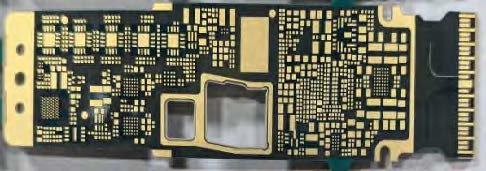
These challenges extend well beyond the optical component itself. The PCB becomes an important part of the system architecture.
As designs become denser, engineers may encounter routing congestion, increasing layer counts, tighter spacing requirements, and limitations on how much circuitry can fit within a given footprint.
The result can be difficult tradeoffs: add layers, increase board size, redesign the architecture—or find a manufacturing process capable of supporting finer geometries.
Is HDI Enough?
HDI remains an important technology for high-density PCB designs, and it is not being replaced by MSAP.
In fact, HDI and MSAP can be complementary technologies. Advanced PCB designs may combine HDI features with MSAP manufacturing techniques to achieve higher routing density and improved performance.
The question isn’t necessarily whether an engineer should use HDI, MSAP, or another technology.
The better question is:
What manufacturing approach gives your design the freedom it needs?
Optical Modules Are Driving PCB Density
As optical networking moves toward higher-speed architectures, the electronics supporting those systems must keep pace.
The market is increasingly focused on technologies and architectures such as:
- 800G optical transceivers
- 1.6T optical modules
- Optical interconnects
- Silicon photonics
- Optical I/O
- Co-Packaged Optics (CPO)
- Linear Pluggable Optics (LPO)
- High-speed networking
- GPU interconnects
- AI fabric and scale-out AI clusters
These are among the key areas identified in MCL’s market roadmap as important terms within the optical module, photonics, and AI interconnect segments.
As these architectures evolve, PCB designs may need to accommodate more circuitry, higher data rates, and greater routing density without proportionally increasing board size.
Where MSAP Enters the Conversation
Modified Semi-Additive Process (MSAP) is an advanced PCB manufacturing process that enables finer trace widths and spacing than conventional subtractive etching.
Instead of removing copper to create the circuit pattern, MSAP selectively builds copper where it is needed. This allows manufacturers to produce finer geometries and higher circuit density.
For the right design, that can provide engineers with additional routing flexibility without simply adding more layers or increasing the PCB footprint.
Potential benefits include:
- Finer Trace Widths and Spacing: MSAP can support significantly finer geometries, allowing more circuitry to fit within the same area.

- Higher Routing Density: More available routing space can help address congestion as designs become increasingly complex.
- High-Speed Signal Integrity: The finer geometries enabled by MSAP can provide additional routing flexibility for controlled impedance designs and high-speed applications.
- Greater Design Flexibility: Engineers may have more options when balancing bandwidth, routing, layer count, and board size.
- Smaller Footprints: By fitting more circuitry into the same footprint, MSAP may allow engineers to reduce board dimensions or add functionality without increasing PCB size.
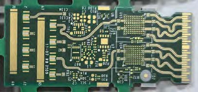
Can Your PCB Manufacturer Hold 20-Micron Traces?
As optical modules, AI interconnects, and high-speed computing platforms become more sophisticated, questions about manufacturing capability become increasingly important.
How fine can your trace widths and spacing be?
How much routing density can your manufacturer support?
Can your PCB accommodate the bandwidth requirements of your next-generation architecture?
And perhaps most importantly:
Can your manufacturing partner support the design intent without forcing your engineering team into unnecessary compromises?
These are conversations worth having early in the design process.
MCL’s Approach: Start With the Engineering Challenge
MCL doesn’t start by recommending MSAP.
We start by understanding what you’re trying to build.
Our team evaluates your engineering requirements, reviews manufacturability early, and works with qualified manufacturing partners to determine the technology best suited for the application.
For some designs, conventional fabrication is still the right answer.
For others, advanced manufacturing technologies such as MSAP can provide the finer geometries, routing density, and signal performance needed for demanding applications.
The goal isn’t to sell a manufacturing process.
The goal is to give your engineering team more design freedom—and keep your program moving.
Built for the Next Generation of Connectivity
The bandwidth explosion driving AI infrastructure and optical networking isn’t slowing down.
From hyperscale data centers and GPU interconnects to silicon photonics, optical modules, and next-generation connectivity, PCB design is becoming an increasingly important part of the performance equation.
MCL provides access to advanced PCB technologies—including MSAP—to help engineering teams navigate these increasingly demanding requirements.
If you’re designing for 800G, preparing for 1.6T, developing optical modules, working with silicon photonics, or pushing the limits of PCB routing density, let’s talk about your design.
MCL can help determine whether MSAP—or another PCB technology—is the right fit for your application.