
Jump To: Copper Filling of Blind Microvias | What Are Microvias? | What Are Blind and Buried Vias? | Advantages of Copper-Filled Blind Microvias | What Are Copper-Filled Vias? | Challenges Associated | Thermal and Electrical Conductivity | The Copper Filling Process | Copper-Filled
Vias, the holes through which stacked pads are electrically connected, are essential parts of printed circuit boards (PCBs). As electronic devices, namely smartphones and other similar products, become more popular and shrink in size, the ability to place smaller vias on the board becomes increasingly useful.
You also need to be able to reliably transfer signals through the layers of the PCB — which can be accomplished by adding a copper layer to the board substrate — but filling the vias with copper provides extra capacity.
Copper-filled blind microvias enable high-density interconnect (HDI) boards and also provide reliable signal transfer. While there are challenges associated with this type of via, they also come with many advantages. Keep reading to learn more about this process and why it may be useful to you.
What Are Microvias?
IPC defines a microvia as a “blind structure (as plated) with a maximum aspect ratio of 1:1…terminating on or penetrating a target land, with a total depth (X) of no more than 0.25 mm [0.00984 in] measured from the structure’s capture land foil to the target land.”
Before its definition was changed in 2013, the term was defined as a via hole smaller than 0.15 mm, or 0.006 inches, in diameter. Over time, that size became more common, and IPC realized it would have to continue to update its definition as vias got smaller if they continued to define using diameter.
Lasers are used to drill holes for microvias, and recent advances in laser drilling have enabled the creation of microvias as small as 15 µm. Although the lasers used can drill through just one layer at a time, PCB manufacturers can produce through microvias by drilling several layers separately and then stacking them.
You’re less likely to encounter manufacturing defects when you’re working with microvias than you would be with normal vias because laser drilling doesn’t result in material being left in the drilled holes. Microvias are, however, just as likely to experience problems with plating and solder reflow.
Because of the small size of microvias, they can be used for high-density interconnect PCBs, which are important today as electronics — especially telecommunications and computing devices — become more advanced but also smaller in size.
What Are Blind and Buried Vias?
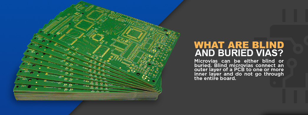
Microvias can be either blind or buried. Blind microvias connect an outer layer of a PCB to one or more inner layer and do not go through the entire board. They connect an outer top layer and the inner layers they reach. Blind vias are useful for increasing wiring density. If you need to route signal tracks from an outer layer to an inner layer, blind vias are often the shortest route for doing so.
Buried microvias connect two or more inner layers and do not reach through to an outer layer. They cannot be seen from the outer layers. Manufacturers usually create them using consecutive laminations.
What Are Copper-Filled Vias?
Copper-filled vias are vias that are filled with either pure copper or epoxy resin with copper. This copper fill enhances the conductivity of the via, helping it to more effectively transfer signals from one side of the board to the other. Many kinds of via can be filled with copper, including standard vias, microvias, blind vias and buried vias.
You can also fill vias with other materials, such as gold, silver, conductive epoxy, non-conductive epoxy and electrochemical plating. The most common type of via fill is non-conductive epoxy. Copper fill, however, provides advantages that make it ideal for certain applications.
Advantages of Copper-Filled Blind Microvias
Using microvias, whether blind or buried, is beneficial for various reasons, including the following.
Space
One of the main advantages of using microvias is that they can save you space, which ultimately results in reduced costs. The more space your vias take up, the more board you need, and the more expensive your project will be.
Microvias are a crucial component of HDI PCBs, which often feature through vias, buried vias, blind vias, coreless construction, passive substrate construction and alternative constructions of coreless builds with layer pairs. In addition to their smaller size and lower weight, these boards also provide enhanced electrical performance due to the reduced distance between components and the higher number of transistors.
Microvias can also help you to utilize via-in-pads (VIPs) more effectively. VIPs save space by creating connections in the pads of surface mounted technologies (SMTs). Because of their smaller size, microvias are well-suited for use with VIPs. Normal vias are sometimes too large to fit inside pads for SMTs. Microvias, however, can fit inside pads with no fabrication issues.
Blind and buried microvias are also easier to fabricate than regular blind and buried vias, which can be difficult to fabricate. Microvias, however, are already made layer by layer, which means it’s easier to make them blind or buried — a process that requires working layer by layer.
Microvias are also useful for breaking ball grid arrays (BGAs). Microvia VIPs can easily fit inside the pads of fine-pitch BGAs. They’re even more beneficial in breakout channels. VIPs save surface space but also require a high number of layers to get outputs to other parts of the board. Microvias can help you increase the width of escape paths, which may enable you to use fewer layers to break out a BGA.
Reduced EMI
Microvias can also help to reduce electromagnetic interference (EMI), which occurs when an electromagnetic field affects an electrical circuit and disrupts the operation of an electronic device. Because they come with a reduced risk of EMI, microvias are especially useful for circuits that are prone to EMI, such as those used in high-frequency or high-speed applications.
High-speed circuits often run into problems with signal radiation and reflection in vias. Reducing the size of the vias, however, reduces the radiation potential, which translates to less EMI. For high-speed circuits, stubs — which are transmission lines or waveguides that are only connected at one end — are another cause of EMI problems. Stubs can reflect signals back into conductors and attenuate or even cancel the original signal. Because microvias are made layer by layer, however, you will not have any stubs.
High-frequency transmission lines, such as microwave and millimeter-wave stripline conductors, require vias to break out signals. Standard vias, however, create too much EMI for use in high-frequency strip lines. Microvias, on the other hand, generate very little EMI and won’t degrade your signal integrity. High-frequency circuits are being used increasingly frequently, making EMI a more common concern.
Filling vias with copper also provides several benefits, namely in the areas of thermal and electrical conductivity.
Thermal and Electrical Conductivity
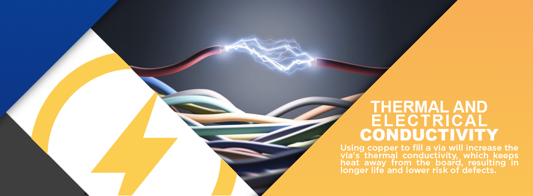
Using copper to fill a via will increase the via’s thermal conductivity, which keeps heat away from the board, resulting in longer life and lower risk of defects. Instead of traveling to different parts of the board, heat will travel through the copper to the other side of the board, protecting its components. Copper has higher thermal conductivity than gold, which is another material used to fill vias.
Copper also has higher electrical conductivity than gold does. The conductivity of the copper in a via will enable currents to cross to deeper layers without overloading the PCB. This feature makes copper-filled microvias ideal for high-voltage applications and those that require strong currents to travel between each side of the board.
Challenges Associated With Copper-Filled Blind Microvias
Certain challenges are associated with fabricating microvias. These challenges can sometimes lead to interconnect defects (ICDs), flaws that occur near the plating and inner copper layer. These ICDs can cause reliability problems, open circuits, intermittent problems at high temperatures and circuit failures. It can be challenging to detect ICDs because they may work correctly during testing after the fabrication stage but then reveal issues during assembly or usage. It’s important to watch for these defects and fabricate boards carefully to avoid them.
Debris-Based ICDs
One common type of ICD occurs because debris ends up in the interconnection hole and then becomes embedded in the inner-layer copper. This debris often results from the hole-drilling process. The lasers used to drill microvia holes do not create nearly as much debris as other hole-drilling processes, so microvias have a lower risk of debris-based ICDs. It’s still important, though, for the manufacturer to check to ensure that all holes are clear of all debris, residue, drill smear, fiberglass, inorganic fillers and other materials before filling them with copper.
Across various types of vias, debris-based ICDs are becoming more common, perhaps because more fabricators are using low DK/low DF materials. These materials are most cost-effective in many ways, but they often create more debris and are more chemically resistant to cleaning than other materials such as standard FR-4 epoxy materials.
Copper-Bond Failure ICDs
Another common type of ICD is a copper bond failure. This type may occur because of high stress during assembly or usage, a weak copper band or a combination of these two conditions. When a copper bond failure ICD occurs, the copper connection physically breaks off. The weaker the copper bond is, the less stress is needed to break it.
The prevalence of copper bond failure ICDs seems to be increasing, possibly because more manufacturers are using thicker PCBs and higher lead-free soldering temperatures. Larger hole sizes and wave soldering can also increase the likelihood of copper bond failures occurring. Copper bond failures occur on microvias as well as standard vias.
Voids and Reliability
Common problems that occur in the copper plating process for microvias include incomplete filling, dimples and voids. These defects can cause reliability issues. According to a study from researchers at the University of Maryland, incomplete copper filling raises the stress levels in microvias, decreasing their fatigue life, which is the number of loading (stress) cycles a specimen can sustain before failing.
The impact a void has on microvia reliability depends on characteristics of the void, such as its size, shape and location. Small, spherical voids, for example, slightly increase the fatigue life of microvias, while extreme voiding conditions significantly reduce their life.
The Copper Filling Process for Blind Microvias
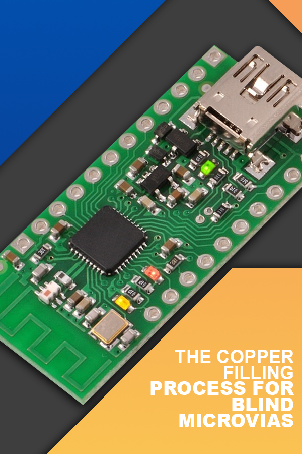
After drilling the microvia holes, the manufacturer will put either pure copper or epoxy resin with copper into them to connect the inner-layer circuits to the PCB surface. This copper enables you to place components or connectors on the board’s surface and allows the circuit to connect between layers.
When working with blind microvias, filling the microvia holes without additives typically results in the formation of voids. The manufacturer always deposits copper until the via is closed, but if additives are not used, less copper is deposited inside the via than on the surface, and voids may form.
Certain organic additives impede the deposition at the surface and help increase plating within the blind microvia, which leads to conformal deposition. Conformal plating also increases the aspect ratio of the blind microvia, which limits the solution and mass transport into it. This process sometimes results in a microvia with a seam in the center.
You can also fill a blind microvia with copper using the bottom-up method, which involves depositing copper preferentially onto the capture pad. This process will ideally create a low dimple combined with a minimum of plated surface copper.
When you’re filling a via hole with copper, it’s important to ensure that the layer of copper within the via is even and that you don’t make the outer layer too thick. Having excess copper adds unnecessary weight to the PCB and may result in having too much copper on the traces. This issue can then result in defects, failure to meet specifications or increased costs, which is even more important with microvias than with regular vias since the design specs are tighter.
An important consideration when filling blind microvias is whether to use pure copper or epoxy resin and copper. Using pure copper is a more traditional method, but this approach can cause voids to form. Contaminants may also get trapped in the copper. Leaving a recess at the top of the filling can help prevent these problems from occurring.
One approach to filling through holes essentially creates two blind microvias. This process involves first using conformal plating and then switching to aggressive pulse plating, which results in the creation of an X-shape in the hole formed by two copper triangles on each hole wall. This shape forms what is essentially two blind microvias, one on each side of the PCB. In the next step, you’ll fill these BMVs completely.
Recent advancements, such as the development of new copper electrolytes, have helped make it easier to fill blind microvias without defects and excess copper. Electrolytes for blind microvia filling often have a high copper concentration, a low sulfuric acid concentration and chloride ions. The organic electrolyte additives used for controlling the coating characteristics typically include a starter, grain refiner and leveler.
Copper-Filled Blind Microvias From Millennium Circuits Limited
Do you need PCBs with copper-filled microvias? We can coordinate the creation of these PCBs and ensure you receive boards made to the specifications you require. We can also supply you with PCBs with a range of other specialized features, surface finishes and base materials. We’ll fill both small orders and large ones with a quick turnaround time.
To learn more about copper-filled blind vias and our capabilities, browse our website, contact us or request a quote today.
![]()