Your Valued HDI Printed Circuit Board Supplier
High-density interconnect (HDI) printed circuit boards (PCBs) are an increasingly integral part of the PCB and electronics industries. Electronic components are becoming smaller and more lightweight but still demand ever-improving performance. To accommodate this, you need to pack more functionality into a smaller area. That’s precisely what HDI PCBs offer.
Get Pricing and Lead Time Call 717-558-5975
What Are HDI Printed Circuit Boards?
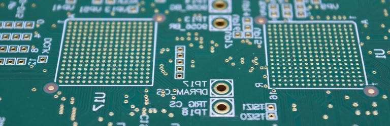
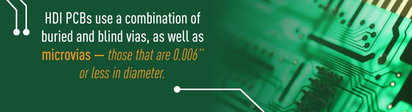
HDI PCBs have a higher circuitry density per unit than conventional PCBs. They use a combination of buried and blind vias, as well as microvias — those that are 0.006″ or less in diameter. High-density circuit boards are PCBs with one or more of the following features:
- Through vias and buried vias
- Through vias from surface to surface
- At least two layers with through vias
- Coreless construction with layer pairs
- Passive substrate constructions that have no electrical connection
- Alternative constructions of coreless builds with layer pairs
HDI technology in printed circuit boards and other areas has been a critical driver for developing many of the electronics we use today, especially those that have decreased substantially in size and weight in recent years. The smaller the equipment gets, the more likely it is to employ HDI technology.
The tight tolerances involved in working with HDI printed circuit boards means you need to partner with an experienced supplier. Even a small defect or layout mishap can cause significant problems. As a leading HDI printed circuit board supplier, Millennium Circuits Limited can deliver top-quality boards that have a significantly higher circuitry density than your traditional PCB.
Benefits of Using HDI Technology
HDI technology provides various advantages over other options that can improve the results of your project. With the right design and the right supplier, using HDI boards in your product can improve its overall quality and performance, as well as your customer satisfaction rate and bottom line. Other advantages include:
- Smaller Size and Lower Weight: With HDI boards, you can secure more components on both sides of the bare PCB, allowing you to get more functionality out of a smaller space and expanding the overall capabilities of the equipment. HDI technology enables you to add functionality while reducing the size and weight of your products.
- Improved Electrical Performance: A shorter distance between components and a higher number of transistors can mean improved electrical performance. These features allow for lower power consumption, which improves signal integrity. Smaller sizes correlate to quicker signal transmissions and more significant reductions in overall signal losses and crossing delays.
- Increased Cost-Effectiveness: With proper planning and manufacturing, HDI boards can be more cost-effective than other options because they require fewer raw materials due to their smaller size and the low number of layers they need. For a product that would have once required multiple traditional PCBs, you may be able to use one HDI board. You’re able to get more functionality and value out of a smaller area and less material.
- Faster Production Times: The ability to use fewer materials — and even fewer boards — combined with design efficiencies linked to HDI technology can translate to faster production times and a shorter timeframe needed to get your product to market. Components are relatively easy to place in HDI PCBs, and the high electrical performance reduces the time needed for testing and troubleshooting.
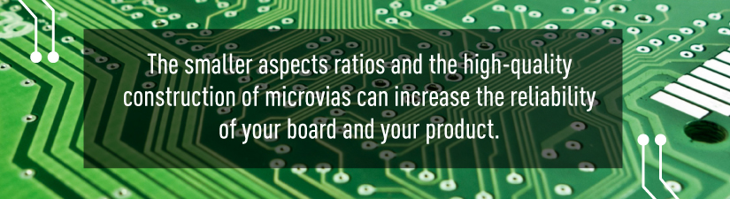
- Enhanced Reliability: The smaller aspects ratios and the high-quality construction of microvias can increase the reliability of your board and your product. The improved performance and reliability HDI PCBs provide will lead to reduced costs and more satisfied customers.
Request a free quote today.

Design Considerations for HDI PCBs
The processes involved in the production of HDI PCBs are often different than those used with other PCB types. Here’s what you need you know about HDI board production and some of the design considerations you’ll want to keep in mind to keep in mind throughout the production process:
- Sequential Lamination: In the lamination process, the PCB core or cores are combined with copper, as well as pre-preg layers for multi-layer PCBs, by applying heat and pressure. The amount of heat and pressure needed varies from board to board. After the lamination phase is complete, the PCB manufacturer will drill vias. Unlike other types of PCBs, HDI boards go through this process multiple times. These sequential laminations help prevent shifting and breaking during drilling.
- Via-in-Pad Process: The via-in-pad production process allows you to place vias in the surface of the flat lands on your PCB by plating the via, filling it with one of the various fill types, capping it and, finally, plating over it. Via-in-pad is typically a 10- to 12-step process that requires specialized equipment and skilled technicians. Via-in-pad is a smart choice for HDI PCBs because it can simplify thermal management, reduce space requirements and provide one of the shortest ways to bypass capacitors for high-frequency designs.
- Via Fill Types: Via fill types should always match your specific application and PCB requirements. Via fill materials we work with on a regular basis include electrochemical plating, silver-filled, copper-filled, conductive epoxy and nonconductive epoxy. The most common via fill type is nonconductive epoxy. You want to choose a via fill that’s flush with the flat land and will solder entirely, just like traditional lands. Fills must allow microvias and standard vias to be blind, buried or drilled, then plated to hide it beneath SMT lands. We often use multiple drill cycles at precisely controlled depths to ensure the drilling process is done right each time. This level of control requires specialized equipment and longer development time.
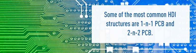
- HDI Structures: HDI PCBs come in a few different layout options. Some of the most common are 1-n-1 PCB and 2-n-2 PCB. A 1-n-1 PCB contains a single build-up of high-density interconnected layers, so it’s the “simplest” form of HDI printed circuit board. It requires one sequential lamination on each side of the core. The 2-n-2 PCB has two HDI layers and allows microvias to be staggered or stacked across layers. Complex designs usually incorporate copper-filled stacked microvia structures. Structures can climb to very high X-n-X levels, though complexity and cost typically limit the buildup. Another important option is the any-layer HDI. This involves an extremely dense HDI layout so conductors on any given layer of the PCB can interconnect freely with the laser microvia structures. These designs appear in GPU and CPU chips in smartphones and other mobile devices.
- Laser Drill Technology: Any-layer HDI designs often require laser microvias created with laser drills. These drills generate a laser at up to 20 microns in diameter, which can effortlessly cut through both metal and glass, creating very tiny but clean holes. You can get even smaller holes by using materials such as uniform glass, which has a low dielectric constant.
- LDI and Contact Imagery: Being a leading HDI printed circuit board supplier means pushing the envelope. MCL can deliver finer lines with cutting-edge technology and clean rooms that ensure safe, secure processing. When it comes to these delicate details, repairs aren’t possible, so it must be done right and with extreme precision the first time. We alternate between contact imaging and LDI imagery based on what’s needed for verifying your equipment. LDI is the go-to for fine lines and minute spacing because it can verify even the most demanding processes, continually expanding our capabilities and allowing for smaller form factors.
HDI PCB Cost Considerations
Many different factors affect the cost of an HDI board. Keep these considerations in mind to determine your budget and ensure your PCB order is as cost-effective as possible:
- Type and Amount of Vias, Through-Holes or Microvias: The via, microvia or through-holes you choose for your HDI PCB will impact its cost, as will the amount of these features you need. Smaller vias cost more than larger ones because they require more precision. Of course, adding more vias can also increase the price.
- Stackup Height and Number of Layers: The type of stackups you need will affect the cost, as well. A 2-n-2 high-density PCB layout is more complicated than a 1-n-1, so it will be more expensive. Additional layers increase the price. You should aim for the most cost-effective and efficient number of layers.
- Materials Used: You may have several choices for the materials your board incorporates. Core materials may be FR4, metal, fiberglass or other material depending on the application. For surface finishes, you can choose between ENIG, HASL, immersion tin, immersion silver, gold and more. ENIG is the most common for HDI due to its flatness and ease of solder ability.
- Number of Sequential Laminations: The number of layers and the number of via structure types determine the number of sequential laminations required. Although more laminations mean more processing time and higher costs, adding more can make improved product performance and cost-effectiveness.
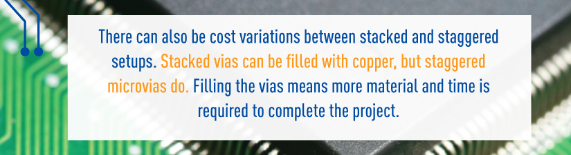
- Stacked vs. Staggered: There can also be cost variations between stacked and staggered setups. Stacked vias can be filled with copper, but staggered microvias do not. Filling the vias means more material and time is required to complete the project.
- Pad Size: You should aim to determine the size of the pad early on to help lower costs. Knowing the proper pad size will help you plan the design efficiently and cost-effectively.
- Turnaround Time: If you request a rush on your board, you may incur higher costs due to the extra resources required to complete a rush order. Sometimes, last-minute situations that come up are beyond your control, but planning orders in advance can help increase cost-effectiveness. MCL offers a quick turnaround time and speedy customer service.
- PCB Supplier: The partners you choose to work with will also significantly impact the cost of your HDI board. You want to select a supplier with competitive pricing that can also efficiently provide high-quality products to ensure cost-effectiveness. It’s better to order a high-quality item once than have to repair or replace components after ordering them.
HDI PCB Industries and Applications
HDI technology is a critical component of many of today’s advanced technologies. The miniaturization of electronic components including PCBs has enabled manufacturers to produce smaller, more cost-effective devices without sacrificing performance or reliability. Here are just a few of the industries that utilize HDI PCBs, as well as how they use them:
- Consumer Electronics: Computers used to take up entire rooms, but now, thanks in part to HDI technology, devices as small as smartwatches are essentially miniature personal computers. You can find HDI boards in laptops, smartphones, tablets and wearables, as well as other consumer electronics like digital cameras and GPS devices. HDI PCBs play a crucial role in enabling the everyday consumer to access these powerful technologies. They’re also essential components of IoT devices for the home, including smart thermostats, fridges and the many other connected devices available. As these smart devices become more common, so do HDI boards.
- Communications: In addition to smartphones and laptops, HDI PCBs also appear in the equipment that allows those devices to function, such as routers, switches, modules and semiconductors. Anytime you use electronic communications, a computerized gadget or a device that uses radio waves, there’s a good chance you’re using an HDI board. Digital video and audio equipment also frequently uses HDI technology. These boards are present in devices used for personal communication, as well as the networks used by businesses.
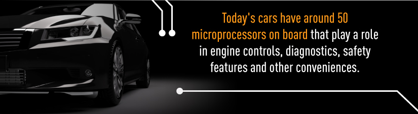
- Automotive and Aerospace: HDI PCBs allow manufacturers to fit more capabilities into smaller spaces and devices that weigh less. This is especially useful in the automotive and aerospace industries, where lower weight can mean more efficient operation. Like almost everything else, cars are becoming more connected and computerized. Today’s cars have around 50 microprocessors on board that play a role in engine controls, diagnostics, safety features and other conveniences. Many new features such as onboard WiFi and GPS, rearview cameras and backup sensors rely on HDI PCBs. As automotive technology continues to advance, HDI tech will likely play an increasingly important role.
- Medical Devices: Advanced electronic medical devices — including some types of equipment for monitoring, imaging, surgical procedures, laboratory analysis and other uses — may incorporate HDI boards. The high-density technology promotes improved performance and smaller, more cost-effective devices, potentially improving the accuracy of monitoring and medical testing.
- Industrial Uses: Industrial equipment is also becoming more computerized, and IoT devices are becoming more common in manufacturing, warehousing and other industrial settings. Many of this advanced equipment employs HDI technology. Today, businesses use electronic tools to keep track of inventory and monitor equipment performance. Increasingly, machinery includes smart sensors that collect usage data and connect to the internet to communicate with other smart devices, as well as to relay information to management and help optimize operations.
Why Choose MCL for Your HDI PCB?
Millennium Circuits Limited has been delivering high-density interconnect printed circuit boards for more than 15 years, and we believe no order is too small, and no tolerance is too tight.Pair that with competitive pricing, quick quotes and response times, domestic and offshore manufacturing and an unprecedented level of flexibility, and you have a winning combination for all your HDI PCB needs.