The last thing any designer wants is to discover last-minute that their product is faulty. Any electronic device is prone to problems, even with proper designs and meticulous building methods. Many electronics come out of the prototype stage with plenty of bugs and issues for their designers to troubleshoot. However, when something goes unnoticed until the product is out in the field, it can mean huge problems for the company.
Testing electronics is so important, especially for printed circuit boards (PCBs), because it prevents several problems from occurring. To get a clearer idea of how testing can improve your products, use this guide to PCB testing methods to learn more about the various processes available.
What Is Printed Circuit Board Testing?
PCB testing and inspection cover a wide variety of printed circuit board testing methods that check if a PCB meets standards, specifications, and requirements.
The primary benefit of PCB testing is to identify problems in the PCB design or manufacturing processes. Whether an issue lies in manufacturability, functionality, or somewhere else, PCB tests identify problems in PCB design and layout, as well as the overall process, so designers can make appropriate adjustments. Thorough testing also prevents wasteful production, reduces the need to scrap full-scale assemblies, results in fewer returned products, and lowers safety risks associated with damage or injury for workers and machines.
There are two major opportunities for testing — prototype and manufacturing testing.
Prototype Testing
Testing for prototypes focuses on making sure a product is producible, will meet the client’s requirements, and performs well. This early life cycle testing provides first thoughts and feedback to designers regarding what works and what doesn’t. Testing in early stages can help save time in the long run by allowing designers to spot major issues during the prototyping stage. During these tests, products face non-ideal situations so teams can learn more about when or where components will break.
Manufacturing Testing
Testing during manufacturing involves verifying that parts function appropriately and the final product is ready for use. Rather than testing a product’s limits, this type of testing often employs many visual and electrical inspections to determine whether a process is reliable and in control. This testing helps ensure that the final deliverable meets customer needs and requirements.
Why PCB Testing Is Necessary
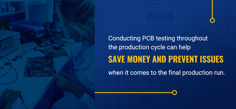
Testing is a crucial part of the manufacturing process for PCBs. Conducting PCB testing throughout the production cycle can help save money and prevent issues when it comes to the final production run. Some industries also adhere to specific regulations requiring certain testing types. For example, the aerospace industry must meet AS9100 regulations, which require verifying that each part conforms to its engineering callouts, such as specified dimensions and characteristics, at appropriate stages of manufacturing and assembly.
You can use some design analysis techniques during the early stages to help minimize major issues during the manufacturing process, but there’s also a wide range of PCB testing methods that can only test physical boards. These tests evaluate potential shorts, functionality problems, and solder joint issues in small-scale assemblies and prototypes to help ensure each board functions as intended.
Types of Printed Circuit Board Testing Methods for Prototyping and Manufacturing
When considering how to test circuit boards, several methods are available, and no single one will catch every problem or meet the requirements of every designer. It’s also important to note that while some testing methods are only useful for either early life cycle testing or manufacturing, some can be used in both scenarios.
Closely consider each testing method to determine if it meets the specific needs of your environment. Some factors to evaluate include the type of product you’re testing, the problems you’re testing for, and the reliability of the test method.
To give you an overview of the testing methods available, we’ve summarized several popular types of PCB testing methods below:
1. In-Circuit Testing
In-circuit testing (ICT) is a popular PCB testing method that many teams use in the later stages of manufacturing, as it can find 98% of faults. This method uses an in-circuit tester, a fixture, and software to complete testing. The tester features drivers and sensors, which perform test measurements. The fixture, which looks like a bed of nails, connects to the in-circuit tester and interacts with the board. Sensor points feed information to the tester via relevant test board point connections. Tester software provides instructions for which tests to perform and dictates the parameters for a pass or fail.
Using the ICT method, a manufacturer can test individual components and measure their performance, regardless of the other components attached to them. Generally, this type of testing is ideal for analog circuits since it’s best at measuring analog measures like capacitance and resistance. Additionally, the cost of the equipment means that this testing method is best for high-volume products. Testing in low-volume applications could be wasteful as designs may change several times.
2. Functional Circuit Testing
A functional circuit test is exactly what it sounds like — it tests the function of the circuit. This type of testing always comes at the end of the manufacturing plan to check whether a finished product meets specifications.
Functional testers come in various forms, each with a primary function to replicate the conditions under which a PCB will operate. These testers typically connect to the board through edge connectors or test-probe points to verify that the board performs as expected according to design requirements.
Typically, this testing evaluates a product’s overall operations, providing a simple pass or fail result. This method doesn’t pinpoint specific faults, making it less suitable for early-stage prototypes needing detailed diagnostics.
This test types shares some similarities with ICT, as both use connectors. However, functional testers rely on pogo pins to make contact and often require fewer connections than a full ICT setup. After connecting to the board, the testing equipment runs programs to verify PCB function.
3. Boundary Scan Testing
Many engineering teams employ the boundary scan test to examine PCB traces. This method is especially useful when it isn’t feasible to access every node directly. This approach involves placing specialized cells at the connection to external pins to assess the board’s functionality.
The boundary scan test sets itself apart from other methods due to its capability to analyze a board without reaching all of its nodes. This feature is crucial for evaluating integrated circuits with complex, multi-layered, or densely-packed layouts — an application which has been increasing in popularity in recent years. Boundary scan testing is also highly adaptable, supporting a range of uses such as system-level diagnostics, memory verification, central processing unit emulation, and flash programming.
4. Automated Optical Inspection
Automated optical inspection, or AOI, uses cameras to capture high-resolution images and verify schematics. This inspection method compares with designs available in the database, allowing you to identify all visible errors with great accuracy. After product placement and soldering, the board will pass through an AOI device. At this point, the advanced camera will capture multiple images, and the system will compare these images to your existing golden standard.
This noncontact method can reduce labor costs while detecting a wide range of surface defects. The nondestructive nature enables manufacturers to reuse or alter components, making it cost-effective. However, in some cases, the system can generate false positives or negatives, highlighting the importance of leveraging high-resolution cameras, setting realistic tolerances, regularly updating reference information, implementing maintenance, and fine-tuning inspection algorithms.
You can include this inspection directly on the production line to compare new products to ideal standards. Technically, AOI is best suited for ensuring correct results from other tests. For example, you can use AOI to verify results from in-circuit tests or flying probe tests. AOI is fast and reliable, but has limitations to what it can capture, highlighting the need for complementary test methods for complete coverage.
5. Resistivity of Solvent Extract Testing
A resistivity of solvent extract (ROSE) test can check for any residue that may remain from solder flux. Fluxes, like potassium fluoride, are essential in solder pastes. However, remaining fluxes on the circuit board can result in corrosion or electrical leakage, leading to failures and malfunctions. It’s critical to characterize the resistivity of the contamination to ensure the quality of soldered parts.
During the ROSE test, the PCB is immersed in a solvent and remains there for a set period. This time allows ionic contaminants to dissolve into the solvent. Testers measure the resistivity of the solvent before and after contaminant extraction to provide insight into contamination. Low resistivity after extraction indicates a high level of ionic contamination, while high resistivity indicates the board is clean. You can compare these results to industry standards and limits to determine if the board passes or fails.
6. Fixtureless In-Circuit Testing/Flying Probe Testing
The flying probe test is a form of ICT that eliminates the need for custom test fixtures, which lower operating costs. This test was first introduced in 1986 and uses a basic fixture to secure the PCB as moveable test pins make contact with specific points as a software-controlled program directs. This method has become increasingly popular since its inception, and many teams in electronic manufacturing rely on it for its versatility.
Fixtureless in-circuit testing (FICT) serves the same general purpose as conventional ICT. One of FICT’s main strengths is the ability to quickly and affordably adapt to new board designs, as teams can make changes by updating the test program. This benefit allows teams to avoid needing to build new tooling, saving significant time and money. However, this method is slower than tradition ICT testing, making it ideal for testing small production batches and prototypes but less suitable for large-scale applications.
7. X-Ray Inspection
Like AOI, these tests capture images to complete the inspection. X-ray inspection can detect errors in solder connections, internal traces, and hidden components with the help of advanced imaging technology. This method allows manufacturers to identify defects early in the assembly process to prevent rework or scrap later.
During this process, the PCB is set in an X-ray machine, which emits X-rays through the board. As the X-rays pass through the PCB, different materials, such as copper or plastic, absorb the rays to varying degrees. A detector captures the X-rays that pass through, creating a grayscale image to reveal internal structures. You can manually or automatically analyze these images to spot defects like hidden solder joint issues, internal layer faults, or misaligned components.
This nondestructive inspection method is beneficial for analyzing hidden components and interior quality. The results are highly detailed. X-ray is most useful for complex and multilayer PCBs, where identifying internal issues may otherwise be difficult. This process is slower than AOI and requires skilled operators for interpretation, but the results can drastically impact assembly processes.
Why Choose Millennium Circuits Limited for PCB Testing?
Regardless of the method you use, PCB testing is an essential step in the design process, helping save your business a great deal of time and money by preventing bugs before they affect your production. However, to successfully run tests on your PCBs, you need a supplier you can trust to ensure your prototypes are made to order every time. MCL can help.
MCL has been supplying bare PCBs for more than 15 years. We’ve become an integral part of customer supply chains and are positioned as a global supplier. Our services adhere to industry-leading tolerance requirements, and we guarantee high-quality production and support services. With quality assurance measures and certifications highlighting our capabilities, you can feel confident in our services.
Work With MCL for PCB Testing
MCL provides several prototypes and small-scale production services that can help speed up your testing process. With incredible reliability and no hidden fees, you can trust us to provide you with high-quality prototypes for your next round of PCB testing. Get a quote today!