Jump To: How do we define Automated Optical Inspection? | The Role of AOI | What an AOI Reviews | How Does AOI Compare With Other Inspection Methods | Contact Millennium Circuits for Thoroughly Inspected PCBs
When you use printed circuit boards (PCBs) in your projects, you need to be sure they’ll perform well and make your clients happy. It’s essential to have a dependable way to test PCBs for flaws and ensure that they function as intended.
Printed circuit boards are becoming smaller and more complex — today’s PCBs may contain thousands of soldered joints and a multitude of tiny components. That increased complexity can give rise to a greater likelihood of errors. When a standard visual inspection is not enough to detect minute imperfections in a densely crowded board, techniques like automated optical inspection (AOI) help provide greater insight and accuracy.
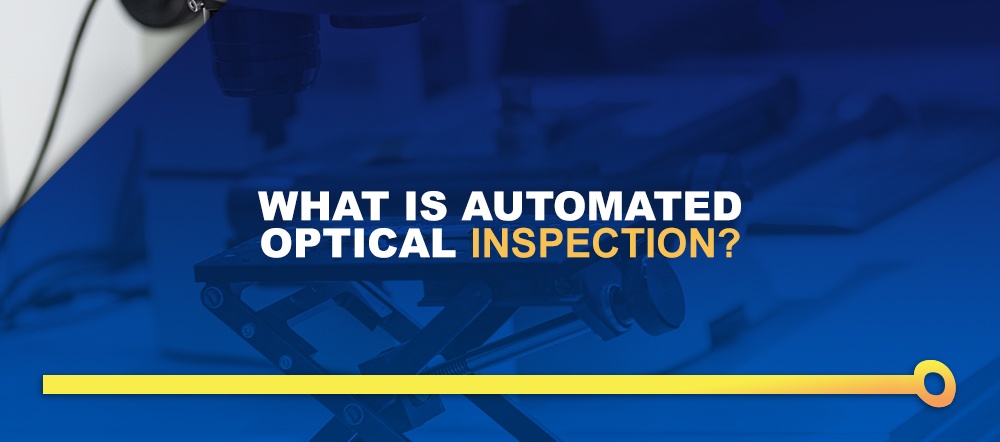
How Does An Automated Optical Inspection (AOI) Work?
How do we define AOI? Automated optical inspection is a visual inspection of completed circuit boards with a machine scanner that uses light imaging. It evaluates the quality of the workmanship to ensure the PCBs are suitable for purchase and use.
An AOI system typically contains many light sources and multiple cameras, sometimes including video cameras. The light sources illuminate a PCB from different angles, and the cameras take pictures or videos to create a comprehensive image for assessment.
AOI measurement generally uses a machine scanner to scan the device autonomously, without the need for human visual inspection. The scanner can check for defects that could cause catastrophic failure — such as the absence of a critical component — and they can also test for smaller flaws that would diminish the PCB’s quality and performance. These smaller defects can include problems such as slightly misaligned components or soldering that forms the wrong size or shape.
AOI is useful at many different production stages. It works well for bare board inspection, solder paste inspection, pre-reflow and post-reflow. Each of these stages can introduce defects into a PCB board’s design, and AOI helps catch them before production proceeds further on a flawed board.
Practically speaking, though, most AOI takes place in post-production. The reason is that AOI can use a single system to inspect for many kinds of defects at the same time. It takes less time to do one comprehensive inspection than it does to inspect after every step in the process. Using AOI as a final check helps the production move faster and allows for higher productivity and deadline meeting. And if AOI turns up flaws in the post-production stage, the defective boards can go back for reworking while the rest of the boards move forward.
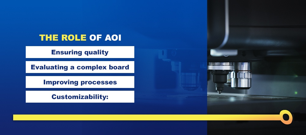
The Role of AOI
AOI plays a critical role in PCB production. It makes sure each board is capable of the high performance required in complex electrical applications.
When AOI uncovers a flaw in a PCB, it flags the board to go back for repairs. This process can happen in a couple of different ways. AOI’s findings may fail specific facility requirements — a requirement that all lines on a board must be over a certain size, for instance. In this case, humans can inspect the findings and determine which boards should return for further work. Or AOI can compare the real PCB to a computer-assisted design (CAD) image of a perfect PCB. AOI can automatically detect places where the actual board deviates from the ideal design and flag it for reworking.
AOI provides the following benefits for PCB production:
- Ensuring quality: AOI allows you to be sure your PCB products function as intended. Ensuring the quality of your products helps you increase customer satisfaction, enhance your reputation in the business and provide peace of mind about the value of the service you’re giving your clients.
- Evaluating a complex board: At Millenium Circuits, if one of our boards contains more than 100 components, it automatically undergoes AOI. AOI can inspect intricate board designs with a degree of accuracy the human eye cannot match.
- Improving processes: If flaws result from faulty processes, catching the flaws immediately via AOI can help you identify patterns of defects and adjust your processes before you turn out thousands of boards with the same faults. A recent study published in the International Journal of Engineering and Advanced Technology reports that catching a fault in a recently assembled board is only 10 times costlier than catching a defect in a bare board, but finding a fault in a board that has gone on to field use is 1,000 times costlier. Catching errors early minimizes the likelihood of future rework and makes your production operations more efficient.
- Customizability: AOI is an automated process, but the operator can set the parameters to tell the scanner what to inspect for. If your design specifications change, it’s easy to adjust your settings to detect the flaws you need to find.
What an AOI Reviews
Below are some of the factors under review during an AOI:
Soldering Defects
Soldering uses a low-melting-temperature alloy, commonly tin and lead or a lead-free alloy, to connect the metal components of a PCB. The process is similar to welding except that it does not melt the metal components. Soldering defects occur when the connections between two metal components fail to form as they should.
Below are a few common soldering defects that AOI can check for:
1. Open Circuits
Open circuits in a PCB are relatively common flaws, and they are problematic because an incomplete circuit prevents the electrical current from running. When a circuit is open, the board will not function correctly.
Open circuits can occur because of improperly formed vias and traces or because of soldering that does not reach its targets. A visual inspection or x-ray imaging can sometimes detect an obvious open circuit, but AOI can identify even slightly open circuits and flag to have the board sent back for proper circuit closing.
2. Solder Bridges or Solder Shorts
Solder bridges occur when solder connects two components on a PCB that should not connect electrically. These bridges can form when board production uses too much solder or when solder seeps into an area of the board intended to remain solder-free.
Solder bridges often occur when the solder does not separate from its leads before it solidifies. The leads are the metal pads designed to connect two locations on the board. The solder may not separate because the leads are so large, or because they have too much paste gluing them to the board, or because the board’s pitch is extremely shallow.
Solder bridges are problematic because they disrupt the intended flow of current through the board. They can cause short-circuiting or burn up critical components or traces on the board. They are also notoriously difficult to detect with the naked eye — even microscopic solder seepage can lead to the formation of a solder bridge. Fortunately, AOI scanning can detect even tiny solder bridges and send the flawed boards back for repairs.
3. Insufficient Solder
An insufficient solder joint occurs when the production process uses too little solder to connect different components to the board. Sometimes the solder fails to connect the components altogether — these situations are known as solder skips.
When the inadequately soldered component connections are unstable, they may not form stable electrical connections, so the board’s performance will be poor. And if the amount of solder is so minute that it cannot hold the components on the board, the board will end up with missing parts, which will most likely result in catastrophic failure. An AOI can scan and note the amount of solder on each component or compare the board to a correct image to determine whether the board requires resoldering.
4. Excess Solder
Excess solder occurs when the opposite happens — the production process puts too much solder onto the board. It sometimes occurs because the soldering tips used are too wide, or it can result from overapplication.
Excess solder can cause many difficulties, including malformations like solder bridges. When production applies too much solder to a pin on the board, it can also create a large round solder ball that makes it difficult to tell whether the pin is sufficiently wetted to stick to the board.
Solder balls are relatively easy to detect because of their size, but a human inspector may miss one after looking at dozens of nearly identical boards. A good AOI scanner can easily detect excess solder and send the board back for reworking with a solder sucker or solder wick.
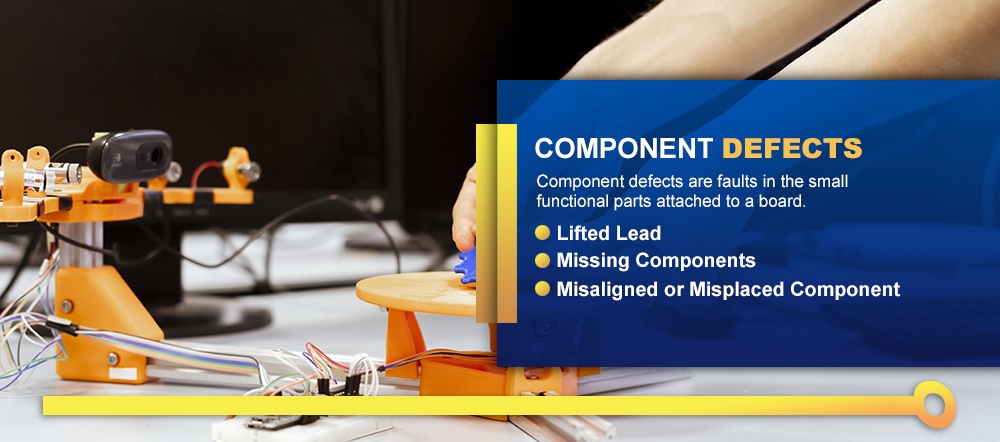
Component Defects
Component defects are faults in the small functional parts attached to a board. Below are a few common component defects on PCBs:
1. Lifted Lead
A lifted lead occurs when one of the tiny metal pads on a PCB fails to adhere properly. Sometimes a lifted lead occurs because of excessive heat or handling during production or because of flexion in the board. Other times it results when leads are too long and rise when they come into contact with solder.
Lifted leads are problematic because they are unstable. The pads on your board allow pins to connect to the copper plate underneath, but if the lead lifts, the pins will not be able to make the proper connections. Missed connections can cause component failure and compromise the board’s performance.
2. Missing Components
A PCB may lack a component for a few different reasons. Inadequate soldering can lead to missing components, or the production process may skip over a necessary part.
A missing component is a serious flaw on a PCB — it is likely to cause catastrophic failure. The human eye may notice missing parts, but because this is such a consequential fault, having a reliable AOI scanner is critical for catching PCBs with missing components before they make it to consumers.
3. Misaligned or Misplaced Component
Misalignment or misplacement can occur when the production process places components incorrectly or when components shift after placement. Component shifting is common during reflow because it’s easy for parts to move atop molten solder — the surface tension of the solder means components can easily slide.
With a misaligned or misplaced component, the PCB may still work, but it may perform sluggishly. Or it could fail to perform at all. Misalignments may be too slight to see with the naked eye, so having a dependable AOI scanner is essential for catching these defects.
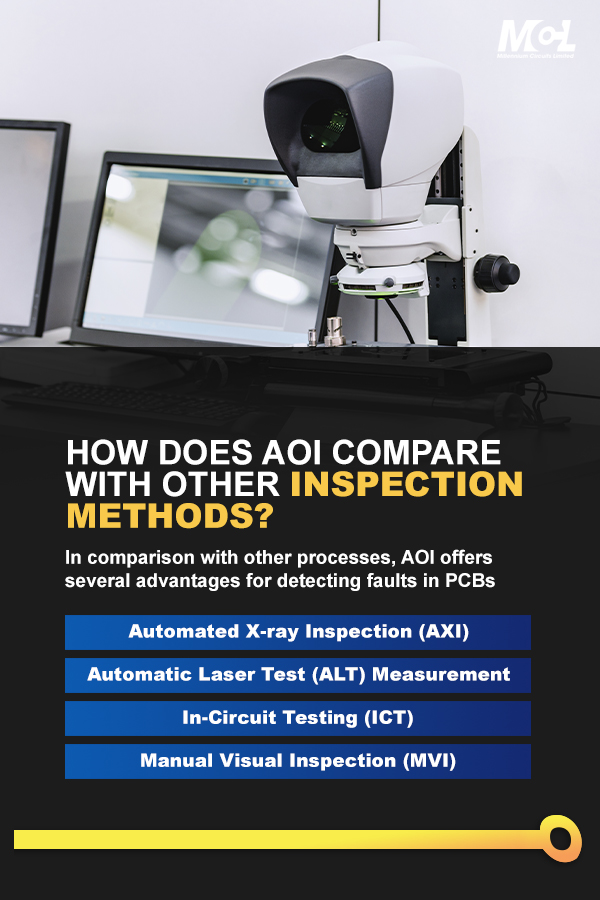
How Does AOI Compare With Other Inspection Methods?
In comparison with other processes, AOI offers several advantages for detecting faults in PCBs. Below is a breakdown of how AOI stacks up against other inspection methods:
1. Automated X-ray Inspection (AXI)
AXI uses X-rays instead of light imaging to inspect the PCBs. Companies often use AXI to evaluate particularly complex or densely constructed boards. The reason is that X-rays travel through the materials to images them. Because the light used for AOI reflects off surfaces, it’s possible for one component to block another. An X-ray travels through different layers of material, though, accurately imaging all of them.
AXI is a new, sophisticated technology, and its main disadvantage is its expense. Because AXI is so costly, it’s often not worth using except with especially complicated or highly clustered boards.
2. Automatic Laser Test (ALT) Measurement
ALT measurement uses lasers instead of traditional light imaging to scan and measure PCBs. As the light from the lasers reflects off the PCB components, the ALT system uses lasers’ locations to pinpoint the positioning and height of different components and assess their reflectivity. As with AOI, the ALT system can compare the empirical measurements to a schematic or set of specifications to detect any flaws.
ALT measurement is particularly useful in evaluating the location and quantity of solder paste, though interference can sometimes make the measurements inaccurate.
3. In-Circuit Testing (ICT)
In-circuit testing uses an electrical probe to evaluate how an assembled PCB will function. It uses an electrical current to check that each component is in place and working correctly. It tests for shorts and open circuits and assesses essential electrical qualities like capacitance and resistance.
Because it uses electrical current rather than imaging, ICT tends to give more limited soldering information than AOI. It can evaluate the quality of electrical components and provide information about soldering defects that affect circuitry, but it cannot offer much detail about insufficient or excessive solder.
AOI is generally more reliable than in-circuit testing, especially for the smaller PCBs being developed today.
4. Manual Visual Inspection (MVI)
Most PCB companies prefer AOI to manual visual inspection because AOI does not require touching the boards. A human inspector must handle the boards, and handling could introduce defects to an otherwise perfect board. AOI can scan PCBs without disturbing their delicate components and preserve their structural integrity.
AOI is also more dependable than human visual inspection. A person can easily miss a small flaw in the PCB. But AOI can catch even the tiniest of errors. Its rigorous acuity never diminishes, it can scan the board in finer detail than the human eye allows, and it is consistently reliable across all stages of the production process.
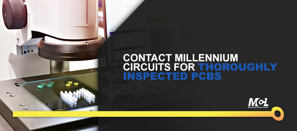
Contact Millennium Circuits for Thoroughly Inspected PCBs
To see the benefits of PCBs that have undergone comprehensive testing and inspection, partner with Millennium Circuits. We supply a variety of different boards, from aluminum PCBs to high current and heavy copper PCBs to specialty boards, so you’ll be sure to get the PCBs that are right for your industry and applications.
Contact us today to learn more.