RF and microwave circuits are now some of the most common PCB designs across the electronics industry, recognized for their abilities to capture higher frequencies than normal circuits. Formerly too costly to make for anything outside of the military and aerospace industries, RF and microwave circuits are now integral parts in a wide range of commercial and professional products, specifically wireless communication devices like cell phones, satellite broadcasters and wireless networks. With higher frequencies, however, come more design challenges.
To ensure these high-frequency RF and microwave circuits are successful, suppliers must consider several RF and microwave design techniques for PCBs.
RF and Microwave PCB Basics
The simplest way to describe RF and microwave PCBs is that they contain components that carry RF or microwave signals. These signals vary in frequency, and the differences in frequency define the differences in components between RF and microwave PCBs and other PCB types. However, grasping the basics of RF and microwave frequencies is the first step to understanding RF PCB design and microwave PCB design.
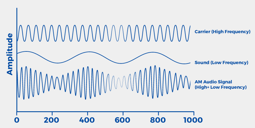
In essence, an electronic signal is a quantity that varies over time and communicates some kind of information. The quantity that varies is usually voltage or current. These signals are passed between devices as a way to send and receive information, like audio, video or encoded data. While these signals are often transmitted through wires, they can also be passed through the air by radio frequency, or RF, waves.
These radio frequency waves vary between 3 kHz and 300 GHz, but they are subdivided into smaller categories for the sake of practicality. These categories include the following:
- Low-Frequency Signals: These are the signals handled by most traditional analog components, and they include signals with frequencies up to 50 MHz.
- RF Signals: While radio frequency, or RF, signals technically cover a wide range of signal frequencies, circuit designers use the term in a narrower scope. Within this field, an RF signal frequency typically ranges from 50 MHz to 1 GHz. These are the same signal frequencies used in AM/FM transmission.
- Microwave Signals: Microwave signals feature frequencies above 1 GHz. The upper limit of these signals is around 30 GHz. These are the same microwaves used to cook our food in microwave ovens. They are also used to communicate very high bandwidth signals.
The signals described above fall within the category of analog signals, though RF and microwave signals are significantly higher than most standard analog signals used in traditional PCB designs. Analog signals are inherently different from digital signals, and each category requires different components to handle their signals. These signals are described in more detail below:
- Analog Signals: An analog signal varies continuously over time, and when you look at this signal on a graph, it shows up as a smooth wave. On this wave, there are an infinite number of value possibilities within a limited range of maximum and minimum values. Most electronic components (resistors, capacitors, transistors, etc.) operate with analog signals, though purely analog circuits are much more difficult to design than digital PCBs. This is mostly because of their susceptibility to noise and other problems. Standard analog signals typically fall between DC and 100 MHz or so, but they vary widely in frequency. RF signals are inherently analog signals.
- Digital Signals: Unlike analog signals, digital signals operate with a finite set of values. The number of values in this set can be very large, but it is not infinite. It’s common to see these digital signals operating with two values, but the signal can only be one of those two values at any one time. When looking at this type of signal over time, the waves created by the change in signals is square, rather than continuous. Digital signals may attempt to replicate the smooth waves of analog signals, but these digital waves will always consist of discrete steps rather than smooth curves. These discrete signals, however, mean digital circuits are easier to design than analog circuits, though they are usually more expensive.
It’s common to find both signals operating within a single circuit, with components designed to convert a signal from one form to another. However, these types of circuits should be carefully designed, especially when the analog components handle high frequency signals like RF signals. The higher the frequency, the more potential there is for problems, like noise.
Common Problems and Solutions for RF and Microwave PCB Designs
PCB layouts with RF or microwave circuits tend to be much more difficult to design than the typical analog or digital PCB. This is because of some of the more problematic features and qualities associated with RF signals. When designing an RF or Microwave PCB, keep the following points and problems in mind.
PCB Design Basics
First of all, RF and microwave PCBs should be designed to minimize any potential for error during the assembly process. Some of the most basic RF layout design guidelines include:
- Keeping Parts Separate: If a board has multiple types of parts, like low-level analog, RF and digital components, they should be kept separate. This is not only easier for the designer to manage, but it minimizes the potential for catastrophic problems during the assembly stage.
- Multilayer PCBs: Ideally, RF and microwave PCBs should include more than one layer. The top layer should include the power stage as well as RF signal lines and components. Be sure that if you have a multilayer PCB, there is a ground layer underneath any layer that includes RF or microwave signal lines.
- Sensitivity to Noise: RF and microwave PCB designers must understand how sensitive these high frequency signals are to noise. While most designers are used to working with such sensitivity in high-speed digital signals, they have to be significantly more cautious with RF and microwave signals, since they are even more sensitive. These signals are also susceptible to a wider variety of noise types. This extreme sensitivity means any possibility signal noise, reflection or ringing has to be mitigated.
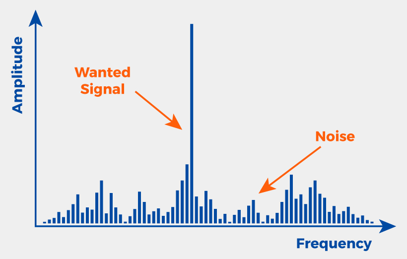
Noise is a term used to describe undesired variations in voltage, which produces errors and functional problems within the circuit. Noise comes in a variety of forms and falls within the following categories according to the distribution of the frequency:
- White Noise: This is a type of noise that adds on to all frequencies equally.
- Pink Noise: Pink noise does not produce a flat response, but instead oscillates with increasing frequency.
- Band Limited Noise: This noise’s frequency band is limited either by the filters or the circuit it passes through.
RF noise can come from a number of sources, which are also categorized according to type. These are described below, along with solutions to each noise type:
- Thermal Noise: Also called Johnson or Johnson Nyquist noise, this kind of noise is the result of thermal agitation. This thermal disruption affects the charge carriers in a conductor, exciting them more than intended, therefore producing noise. Such problems can usually be solved by minimizing the effects of temperature on the circuit, often by regulating the temperature through cooling systems around the circuit or heat-dissipation features on the circuit itself.
- Shot Noise: This noise comes from the fluctuations in electrical current over time, caused by the discrete nature of electron charges. Since this noise is caused by current flow, it’s difficult to be rid of, though metallic resistors tend to minimize their occurrence. Fortunately, shot noise is only apparent in devices like tunnel junctions and barrier diodes.
- Phase noise: This type of RF noise is visible on radio frequency signals, and it can significantly affect the performance of a system. This noise appears as phase jitter, or fluctuations, within the signal itself, which manifests as sidebands spreading to each side of the signal or carrier. This can be a particularly problematic type of noise when carrying digital information, as phase noise can degrade the bit error rate and, therefore, the quality of the data being transmitted. Cleaner signals are the best way to reduce this noise, which must be accounted for early in the design process.
- Flicker Noise: Also called 1/f noise, this noise occurs in almost all electronics and is usually caused by the direct current flow. It is proportional to the inverse of the signal frequency, but it manifests similarly to phase noise. Processing the signal through a specialized filter will usually help reduce this kind of noise.
- Avalanche noise: This noise is caused by a junction diode operating too closely to the point of avalanche breakdown. The result is a lot of noise produced at the diode. Removing this avalanche noise is as simple as using a capacitor based filter or smoothing network.
A lot of noise can be mitigated with appropriate band pass filters, which transmit the signals in a “band of interest.” Only signals within a specific frequency range can pass through this filter, while the filter blocks the rest. However, this does not solve the problem of inaccurate signals within the frequency range. Ideally, the source of the noise should be removed through one of the above methods.
Impedance Matching
Impedance matching is another important requirement for RF PCBs. While high-speed digital signals are somewhat tolerant when it comes to impedance matching, the higher the frequency, the smaller the tolerance. With RF and microwave signals, this tolerance is particularly tight.
There are several things to keep in mind when you’re considering impedance matching in your design. These include the following:
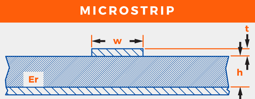
- Skin Effect Loss: At higher frequencies, electrons will start to flow along the outer surface of the conductor. This is called a “skin effect.” At the trace, a small area is used to funnel electrons. However, this funnel also traps some of the electrons flowing on the outside of the conductor, converting their signal energy into heat. This is what is called “skin effect loss.” This loss is best minimized with proper impedance matching and even PCB plating with gold.
- Keep Line Lengths Low: The longer the lines that carry RF/Microwave signals, the more chance there is for signal loss. Ideally, the line should be 1/20 of the wavelength. If it needs to be longer than 1/16 of the wavelength, also called the critical signal length, you’ll need to apply impedance control to that trace with L and C components to the end of the line.
Return Loss
Return loss is often caused by signal reflection. Unfortunately, since RF and microwave signals are more sensitive to signal noise, return loss is a more prominent problem. While return signals usually follow the path of least resistance, higher frequency signals tend to take the path of least inductance. Such paths tend to include the ground planes beneath the original signal.
To minimize return loss, ground planes should be continuous from the driver to the receiver, otherwise the return signal could pass through other power planes. Since these alternative paths are less ideal, they can cause significant signal noise through reflection and ringing, or even be lost in the form of heat.
Crosstalk
Crosstalk is an unintentional transfer of energy between conductors, resulting in a coupled signal. Such a transfer is usually the result of mutual inductance and shunt capacitance, and the incidence of crosstalk tends to increase as the density and performance of a PCB increases. The proximity of the conductors, the distance over which they run parallel and the edge rate of the active line also play a significant role. Crosstalk tends to be a serious issue for high frequency designs, like RF and microwave designs, which is why designers must do what they can to prevent crosstalk.
Crosstalk should be minimized as much as possible. Fortunately, there are multiple ways to do so. These methods include:
- Separating Signals: The distance from center to center should ideally be around four times the trace width of the signals.
- Minimize Parallel Lines: If the lines absolutely have to run parallel to one another, keep the distance over which the lines run parallel to one another to a minimum.
- Reduce the Dielectric Spacing: The dielectric spacing between a line and its reference plane should be minimized.
- Introduce a Co-Planar Structure: Insert a ground plane between the traces.
- Terminate the Line: Ending the line on its characteristic impedance can reduce cross talk by as much as 50 percent.
Laminate Properties
The properties of a PCB laminate can have a significant effect on the functionality of an RF or Microwave PCB. FR4, for example, has a higher dissipation factor than high-frequency laminates, meaning FR4 laminates can result in higher insertion losses as signal frequencies increase. Additionally, the dielectric constant, or Dk value, of FR4 tends to be higher and more variable than that of high frequency laminates. FR4 Dk values can vary as much as 10 percent, which in turn varies the impedance.
Dielectric loss is a common problem associated with the properties of the laminate. Similar to skin effect loss, dielectric loss occurs when electrons flow through a conductor and bounce off the electrons of the FR4 PCB substrate. During the interaction of these electrons, some of the signal energy from the flowing electrons is transferred to the FR4 electrons, which in turn convert the energy into heat. This kind of loss can be avoided by using substrates with very low dissipation factors, like polytetrafluoroethylene Teflon, which has a dissipation factor around 0.001 as opposed to FR4’s dissipation factor of 0.02.
Get More From Your PCB Designs with Millennium Circuits Limited

If you want to learn more about PCB Designs, or if you want to find a top-rated PCB supplier, Millennium Circuits Limited (MCL) is the best choice in the industry.
Since 2005, MCL has dedicated itself to quality PC board fabrication, and now, more than ten years later, we still dedicate ourselves to that goal. Today, MCL is the newest privately owned, ISO-9001 certified high-volume PCB board fabrication company based out of Harrisburg, Pennsylvania. Our goal is as simple now as it was when we started — produce the best PCB every time. Whether you need a small prototype batch or a high-volume PCB order, we can get it done quickly and with the highest product quality possible. We have manufacturing facilities across the globe, allowing us to create your PCBs according to your budget and timeframe.
When you partner with MCL, you work with a company that strives to give you the best service possible, building our relationship with you so you can feel comfortable working with us. As of today, MCL has achieved a 98% satisfaction rating among its customers, with 99% of our deliveries arriving on time. That’s why more than 400 companies across the globe choose to work with MCL over any other PCB supplier company.
To learn more about what MCL can do for you and your next PCB, contact us today.