In today’s computerized and mobile-activated world, signals are sent between numerous devices. To enable each command, two or more circuit boards must establish a connection. None of this would be possible without gold fingers, which serve as the connecting contacts between motherboards and components like graphics or sound cards.
The technology used to transmit these signals and commands is a huge leap forward from earlier electronics, which typically consisted of separate modules that were difficult to bring into communication with one another. With gold fingers, the main processing board can immediately read the processes of another circuit board.
The processes associated with this advanced technology extend across all corners of the public and private sectors. In the world of manufacturing, signals are sent between various devices and machines to enact a series of processes, many of which could not be carried out by human hands. At auto-assembly factories and food-packaging plants, computer-prompted machinery, most of which use circuit boards of one size or another, fulfills numerous commands.
Many of today’s industrial processes are made possible by gold fingers. So what are they, and why are they so important to the inner workings of computer technology?
What Are PCB Gold Fingers?
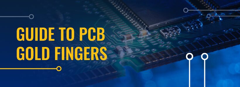
The gold-plated columns along a printed circuit board’s (PCBs) connecting edges are gold fingers. These components aim to connect secondary PCBs to a computer motherboard. PCB gold fingers are also used in various other devices that communicate via digital signals, such as consumer smartphones and smartwatches. Gold offers stable, low-contact resistance and high conductivity, making it ideal for usage on a PCB’s connecting points.
The PCB gold finger plating process leverages two approaches:
- Electroless Nickel Immersion Gold: This surface finish, known as ENIG, is easier to solder and generally more cost-effective than electroplated gold. However, it is also soft and thin, and a 2-5 microinch (µin) composition can render it unsuitable for PCBs that face abrasive effects from insertion and removal.
- Electroplated Hard gold: Electroplated hard gold is solid and thick, often 30 µin. These characteristics make it ideal for the abrasive effects of constant PCB usage.
Gold fingers enable one circuit board to communicate with another — to carry out a command, electrical signals travel from the power source through multiple contacts to the intended system or device.
When you initiate a command, the signal may move across one or more boards before interpretation begins. For example, pressing a remote function on a mobile device sends a signal from the PCB in the phone to another machine, where that machine’s circuit board receives and processes the signal.
Creating reliable gold fingers requires a tightly controlled plating process that requires several careful steps. This process ensures that each board leaves production with the ability to transmit signals accurately. Following established plating standards also helps the fingers align and mate precisely with the matching motherboard slots.
Each PCB must pass a series of inspections and defect tests to confirm that contact fingers and mating slots align with tight tolerances. If a gold layer is uneven or doesn’t have a proper bond to the substrate, the board will not meet commercial quality standards.
Forming PCB gold fingers is a staged process, and you must complete the surrounding board features first. When it’s time to plate the contacts, manufacturers will deposit a nickel barrier over the copper and follow with a final surface finish. Once everything has set, the board is inspected under a magnifying lens and subjected to adhesion tests, like the ASTM B571.
How Gold Fingers Are Used
Gold fingers connect two adjoining PCBs. Gold offers conductivity and can protect the connecting edges from wear over many uses. Hard gold’s strength at a specified thickness ensures gold fingers allow a PCB to connect, disconnect, and reconnect up to 1,000 different times in a corresponding slot.
The functions of gold fingers are multipurpose. With any given computer setup, you will see a number of peripherals that connect with the computer itself, thanks to PCB gold fingers. Some of the most widespread uses of gold fingers include the following:
- Interconnection points: Several female slots connect secondary PCBs to the main motherboard. These slots, like AGP, ISA, or PCI/PCIe slots, allow gold fingers to conduct signals between peripheral devices and the computer.
- Special adapters: Gold fingers enable users to enhance personal computer performance. Through secondary PCBs that slot perpendicular to the motherboard, a computer can deliver enhanced graphics and hi-fidelity sound. Since these cards are seldom unattached and reattached, the gold fingers generally outlast the card itself.
- External connections: Monitors, printers, scanners, speakers, subwoofers, and other devices in a computer station all plug into specific slots at the back of the computer tower. These slots, in turn, attach to PCBs that connect to the motherboard.
For the corresponding device to work, its own card must connect to a power source. The fingers and corresponding slots on the motherboard make this possible. Gold fingers provide module PCBs with the power to operate and deliver modern-day functionality to users of remote and stationary computing devices.
The flexibility of the PCB system, whereby different slots connect different types of cards, makes it possible to upgrade the same computer periodically over five or 10 years. Every time a sound or graphics card receives an update, you can remove the preexisting card from your motherboard and replace it with the new and improved model. Through each update, the PCB gold fingers remain the universal connecting contact.
Beyond the realm of personal computers, PCB gold fingers also act as the connecting contacts in computerized industrial machinery. The large arsenals of mechanized equipment that you would see at a pressing plant or automotive factory will include an assortment of internal cards that connect to a main source of power via gold fingers. Factory robot arms, for example, leverage gold finger cards that prompt an assortment of movements.
PCB Gold Finger Guidelines to Note
During the PCB gold finger plating process, manufacturers must adhere to certain standards to ensure proper finger function. The design of the PCB itself must also account for the areas needed for proper finger length and alignment. Regardless of the purpose or size of the PCB itself, the following PCB gold finger design rules are always applicable:
- Do not place plated through-holes close to gold fingers.
- Prevent contact between gold fingers and screen printing or solder mask.
- Ensure the fingers face opposite the middle of the PCB to achieve a beveled edge.
If manufacturers do not adhere to any of these rules during the PCB gold finger plating process, the PCB might be incapable of communicating with the parent circuit board or might not fit properly into the appropriate slot on a motherboard.

Why Use Gold for PCB Connecting Fingers?
The reason why gold is used on PCBs is due to the alloy’s superior strength and conductivity. Although gold is more expensive, it is an essential component for meeting PCB function requirements. Using more available, cost-effective metals like nickel or copper may result in oxidation and high contact resistance.
PCB gold finger durability and strength make it possible to inject and eject the fingers hundreds of times without wear to the connecting contacts. Without the protection of the gold plating, a few uses could easily strip a circuit board of its connecting functions.
As PCB technology matured, gold became a preferred contact material for several reasons — namely, its excellent conductivity and strong corrosion resistance. The gold in PCBs is also often alloyed with other materials to add strength and improve durability. Materials like nickel and cobalt can enhance wear resistance, making them suitable alloys for frequent-use applications.
The Association Connecting Electronics Industries (IPC), accredited by the American National Standards Institute (ANSI), first established production standards for PCB gold fingers in 2002, with the most recent update in 2015. IPC A-600 and IPC-6010 remain the most widely employed standards for gold connecting fingers in the industry. These IPC standards cover:
- Chemical composition: Gold plating should consist of 5-10% cobalt for maximum rigidity along the edges of PCB contacts.
- Thickness: Standard thickness sizes for gold fingers are 0.125, 0.093, 0.062, and 0.031 inches. The gold finger plating thickness of gold fingers should always be within the 2 to 50 microinches range. Prototypes often use lower thicknesses, while connecting edges that face regular insertion and unplugging use higher thicknesses.
- Visual test: Visual tests with a magnifying glass can verify gold fingers. Edges should not have the appearance of nickel, be free of excess plating, and possess smooth, clean surfaces.
- Tape test: The IPC recommends testing the adhesiveness of the gold plating and the contacts using the tape test, as specified in IPC-TM-650. During this process, testers will use a strip of tape to determine whether there is a presence of plating. If any gold plating is evident on the tape, the plating and contacts lack sufficient adhesion.
Numerous other standards exist for the PCB gold finger plating process, and all should be read in full for an in-depth understanding. As technology improves, further standards of testing are commonly introduced to the process, so it is best to check back with the IPC for updates periodically.
Gold Finger Plating and Beveling Process
On a circuit board, the PCB gold finger plating process is used after the solder mask and before the surface finish. The plating process generally consists of the following steps:
- Nickel plating: Plate between 3 and 6 microns of nickel to the connector edges of the fingers.
- Gold plating: Between 1 and 2 microns of hard gold plating rests over the nickel. Cobalt usually enhances the gold for better wear resistance.
- Beveling: Specified angles enable easier insertion. It’s common to bevel PCB edge connectors between 30 and 45 degrees.
Some circuit boards have gold fingers of varying lengths. In some cases, having longer fingers at one end can make it easier to insert the PCB into a slot. The longer fingers will snap into place, and the user will only need to push the other end into position.
There are certain restrictions to the plating process. For example, certain distances are necessary between the gold fingers and other parts of the circuit board. Key restrictions include the following:
- Inner layers must be copper-free along the PCB edge to prevent copper exposure during the beveling stage.
- Plated holes, SMD, and pads should not be within 1.0 millimeters of the gold fingers.
- Plated pads cannot exceed 40 millimeters in length.
- A distance of 0.5 millimeters should exist between the gold fingers and the outline.
Any deviation from the standard spacing requirements around the gold fingers on a printed circuit board could result in a physically weak or dysfunctional card.
How Gold Fingers Are Changing the World
Today’s computers and mobile devices are growing more complex as manufacturers compete to make their products faster and more resourceful. If you build a large computer station and amass a handful of mobile devices, you are liable to have numerous gold-plated circuit boards interacting at the same time. Each time you print out an article or scan a photo to upload to a social media account, peripheral devices send signals to motherboard cards, which receive these signals via PCBs.
Thanks in large part to gold fingers, technology has advanced to the modern array of mobile devices that millions now use on a daily basis. Moreover, gold fingers have allowed industries to become more productive and capable than ever before.
Why Trust Millennium Circuits Limited (MCL)?
MCL has been supplying customers with bare PCBs for more than two decades. Our capabilities empower teams to navigate manufacturing complexities. As an ISO 9001:2015-certified company, MCL has proven its ability to implement the necessary controls and processes to ensure consistent quality.
Our domestic and offshore capabilities ensure we can meet the needs of a diverse customer pool. Our strategic manufacturers use a personal approach and leverage thorough assessments to meet customer expectations and industry standards. We make it easy to find an optimal PCB supplier. Our team can assist with everything from prototyping to finishing, empowering you to access competitive prices and high-quality work to remain competitive in your industry.
Partner With MCL
As increasing amounts of technology rely on gold fingers, it is crucial to have them plated and tested to the highest standards. Only this way can you ensure maximum performance without fail from the tech products that use circuit boards. At MCL, we provide PCBs of the highest quality for customers in a variety of industries. Contact us today for a free quote.
