
One of the critical factors that impacts the performance and reliability of your printed circuit board (PCB) design is the width of the traces. Incorrectly sized circuit board traces can lead to unreliable performance or complete failure.
Whether routing for high-current applications or dealing with high-frequency signals, getting trace width right is nonnegotiable. A PCB trace calculator can help determine the ideal trace width for specific conditions.
Why PCB Trace Width Matters
PCB traces are the copper lines etched into the board that carry electrical signals and power between electronic components. Engineers must size these traces precisely to meet the circuit’s electrical and thermal demands.
Improper trace sizing can result in:
- Thermal overload: An undersized trace can cause localized heating, which might damage surrounding components or the PCB itself.
- Voltage drop: Resistance increases along narrow traces, causing uneven power distribution.
- Signal degradation: High-frequency signals may reflect, distort, or couple into adjacent traces if routing isn’t well-managed.
- Unnecessary complexity: If a trace is too wide, it may impact impedance control and unnecessarily increase the size and complexity of the board.
What Is a PCB Trace Width Calculator?
A PCB trace width calculator is a tool or formula that helps designers predict how a trace will behave under electrical load. With variables such as copper thickness, current load, desired temperature rise, and trace length, you can calculate parameters like:
- Maximum current capacity
- Voltage drop across the trace
- Power dissipation
- Trace resistance
Factors Affecting Trace Width
Several variables influence the required trace width for safe and efficient operation:
- Current requirements: Higher current demands require wider traces to reduce resistance and dissipate heat effectively.
- Desired temperature rise: The maximum acceptable temperature rise determines how much thermal stress the trace can safely endure. In common consumer electronics applications, IPC-2152 guidelines recommend limiting this rise to 10 degrees Celsius above a 25 degrees Celsius ambient temperature.
- Copper weight (oz/ft²): Also called copper thickness, this affects how much current a trace can carry. Heavier copper can handle more current.
- Ambient temperature: Higher ambient temperatures reduce the thermal margin available for trace heating.
PCB Trace Width Calculator: Formulas and Calculations
The formulas below are essential for calculating the optimal PCB trace width as per ANSI/IPC-2221/IPC-2221A standards.
PCB Trace Width Current Calculator
The maximum current that can flow through the trace depends on the trace’s cross-sectional area. Here are the steps for calculating maximum current:
1. Cross-sectional area
To calculate the cross-sectional area (A) of a trace, use the formula:
A = T × W × 1.378
Where:
- A: Area in mil²
- T: Copper thickness (oz/ft²) (converted to mils)
- W: Trace width (mils)
- 1 oz/ft^2 = 1.378 mil: A constant for unit conversion
2. Maximum current
Once you have the trace’s cross-sectional area, you can calculate the maximum current a trace can carry as follows:
IMAX = (k × TRISEᵇ) × Ac
Where:
- IMAX: Maximum current in amps
- k, b, c: Constants resulting from curve fitting to the IPC-2221 curves
- TRISE: Maximum desired temperature rise (°C)
- A: Cross-sectional area of the trace (mils²)
Trace Temperature
The trace temperature is the maximum temperature at which the trace can operate safely. It’s a critical factor when determining trace width:
TTEMP = TRISE + TAMB
Where:
- TTEMP: Trace temperature (°C)
- TRISE: Maximum desired temperature rise (°C)
- TAMB: Ambient temperature (°C)
Trace Resistance Calculator
Resistance along a copper trace contributes to voltage drops and power loss. It is an essential variable when determining PCB trace widths. Follow the following steps to calculate resistance:
1. Convert area from mils² to cm² since resistivity is in Ω·cm
A’ = A × 2.54 × 2.54 × 10⁻⁶
Where:
- A: Cross-sectional area in mil²
- A’: Cross-sectional area in cm²
2. Calculate resistance using the formula
R = (ρ × L / A′) × (1 + α × (TTEMP – 25))
Where:
- R: Trace resistance in ohms (Ω)
- ρ: Resistivity of copper (~1.72 × 10⁻⁶ Ω·cm)
- L: Trace length (cm)
- A’: Cross-sectional area (cm²)
- α: Temperature coefficient of resistance for copper (~0.0039/°C)
- TTEMP: Trace temperature (°C)
Voltage Drop Calculation
Voltage drop is the decrease in electrical potential as it moves through a current in an electrical circuit.
The equation for determining voltage drop is:
VDROP = IMAX × R
Where:
- VDROP: Voltage drop in volts (V)
- I: Maximum current (A)
- R: Trace resistance (Ω)
Calculating Power Dissipation
Power lost as heat due to resistance is another critical consideration:
PLOSS = R × I2
Where:
- PLOSS: Power loss in watts (W)
- R: Resistance (Ω)
- I: Maximum current (A)
Important note: Based on the formulas, the tool can only calculate trace width of up to 400 mils, 35 amps, copper of 0.5 to 3 ounces per square foot, and a temperature rise between 10 and 100 degrees Celsius. The calculator will extrapolate the data when used outside these ranges.
Understanding Trace Impedance
Impedance refers to the opposition that a circuit presents to the flow of alternating current (AC), and it’s influenced by the frequency of the signal, the trace’s geometry, and the surrounding dielectric material. For most standard applications, impedance is not a significant concern. However, controlling the impedance becomes critical for high-speed digital circuits or high-frequency analog circuits to avoid signal reflections, transmission loss, or data errors.
How Impedance Works
Every PCB trace contains distributed inductance and capacitance along its entire length:
- Inductance: Inductance (L) is the property that opposes rapid changes in current flow. Each trace generates inductance based on its geometry and layout.
- Capacitance: Capacitance (C) is formed by the electric field between the trace and its nearest return path, usually a ground plane. It depends on trace width, the dielectric constant of the PCB substrate, and spacing.
Together, inductance and capacitance create a distributed LC circuit along the trace. As signal frequencies and rise times (how quickly a signal transitions from low to high) increase, impedance effects become more pronounced. The rise in impedance occurs because signals with shorter rise times behave like AC signals, making impedance a critical design factor in such scenarios. When impedance is not intentionally managed, it’s called “uncontrolled impedance.”
Controlled Impedance
Controlled impedance is a technique engineers use to prevent signal integrity issues at high frequencies by maintaining a consistent impedance value along the trace. It’s essential in applications such as:
- High-speed digital buses such as PCIe, USB, and HDMI
- RF communication systems like GPS, Wi-Fi, and cellular networks
- Precision analog circuits and video signals
Controlled impedance is achieved by calculating and precisely managing the following parameters:
- Trace width: Wider traces generally have lower impedance.
- Trace thickness: Thicker traces have lower impedance.
- Spacing to reference plane: A closer ground/reference plane reduces impedance.
- Dielectric constant (εr): Materials with a higher dielectric constant will result in lower impedance.
- Laminate thickness: Adjusting laminate thickness influences impedance.
Stripline vs. Microstrip
PCB traces typically follow two main transmission line designs:
- Microstrip: In this configuration, the trace is located on the surface layer of the PCB. Microstrips are simpler and less costly to manufacture but have more radiation loss than striplines.
- Stripline: In this PCB layout, traces are located on internal layers of the PCB, sandwiched between two reference planes. Striplines offer improved signal isolation, reduced EMI, and more stable impedance control. However, they’re more complex and costly to manufacture.
Trace Impedance Calculator
The IPC-2141 formulas below provide a reliable starting point for impedance control. These empirical models simplify initial trace sizing. However, more precise methods, such as Wadell’s equations or artificial intelligence (AI) and machine learning techniques, may be necessary to refine final adjustments.
These equations are only accurate for a target impedance of 50 ohms.
Microstrip Formula
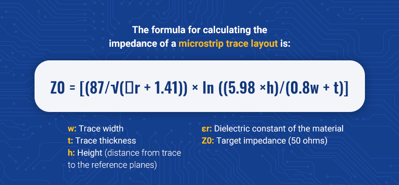
The formula for calculating the impedance of a microstrip trace layout is:
Z0 = [(87/√(εr + 1.41)) × ln ((5.98 ×h)/(0.8w + t)]
Where:
- w: Trace width
- t: Trace thickness
- h: Height (distance from trace to the reference planes)
- εr: Dielectric constant of the material
- Z0: Target impedance (50 ohms)
Important note: The microstrip formula provided above is only valid if the ratio of trace width to height is between 0.1 and 2.0.
Stripline Formula
The formula for calculating the impedance of a stripline (symmetric) trace configuration is:
Z0 = [(60/√εr) × ln (1.9(2h+t)/(0.8w+t))]
Where:
- w: Trace width
- t: Trace thickness
- h: Height (distance from trace to each reference plane)
- εr: Dielectric constant of the material
- Z0: Target impedance (50 ohms)
Why Trust Millennium Circuits Limited (MCL)?
At MCL, we’ve been helping engineers meet trace width and impedance goals since 2005. As a global supplier of printed circuit boards, we offer solutions tailored to your specific PCB layout and performance requirements.
Working with MCL provides several benefits:
- Expert technical support: MCL offers detailed design for manufacturability analyses, cost consulting, and life cycle management to optimize your designs and budgets.
- Comprehensive capabilities: From prototypes to high-volume production, including metal core, rigid-flex, and ceramic-core PCBs, we handle it all.
- Proven quality: Our ISO 9001:2015-certified processes and adherence to IPC-A-600 standards ensure consistent, reliable performance.
- Personalized service: Our dedicated customer concierges ensure clear, timely communication and a tailored experience for every project.
Use Our Trace Calculator for Your PCBs Today

Accurate trace width and impedance calculations ensure optimal signal integrity and heat management in PCBs. MCL empowers engineers with the tools, expertise, and technical support to design PCBs that meet precise performance standards.
Whether you need rapid prototyping or production-grade multilayer solutions, we have the knowledge and resources to support your design needs and provide high-quality, custom PCBs for your applications. Contact us today to learn more.